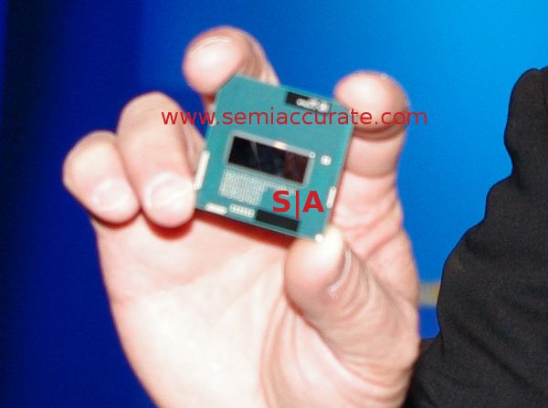
 At IDF last week, Intel’s (NASDAQ:INTC) Mooly Eden held up a Haswell chip, or part of one from the look of things. This isn’t to say that Intel was trying to fake anything, they weren’t, they were just hiding a few secrets here and there.
Unlike the wood screws at Nvidia, Intel was quite clear that the part that was held up was not functional or complete. This isn’t to say they don’t have such a part, there was one running demos about 20 feet to the right of Mooly while he was waving it around, and a few more sprinkled around at IDF.
There were however some selective omissions for the sake of not tipping off the competition to Intel’s technological lead, and it is huge, the technological lead, that is. If you look at the chip, you can see several things even through our awful photography. These are the best ones we took, but for all of his skill as a world class hand model, Mooly does move quite a bit. It is going to be a while before he masters “Blue Steel”.
The front of Haswell
Looking at the front of the chip, a few things are immediately evident. The first is the odd shape of the chip. It is really rectangular, not the normal square you would want if you are looking at manufacturing costs. Sources tell us that this is the ‘big’ Haswell, and the shaders take up most of that die. They also say that there are options “above GT2, but no real plan of record has been finalised yet” for the GPU, and this is likely that “above GT2” part.
That is not the interesting bit though. Look at the passive components, the caps, resistors, and other things that look like blurry dots around the edge of a CPU. Notice how they are arranged? They are all clustered on one corner of the package, with a few outliers. This isn’t a normal layout.
Sane CPU packagers would spread those components out around the PCB/package. This eases power delivery and makes signal routing much easier. Since this type of routing is one of the, if not the major problems in laying out a modern CPU, well, you just don’t lay things out like this. If you look at just about every other CPU out there, the production parts, not the lidless photo models, you will see a nice even spread of the passive components. Sometimes a manufacturer will put them on the underside of the package too, but the layout is not wildly asymmetric. If you look at the back side of the Haswell die, you see something interesting too.
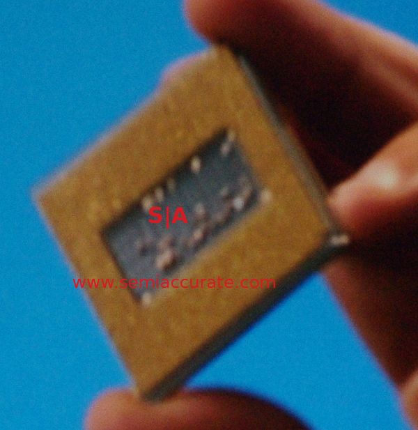
The back of Haswell
The first thing you notice is that there aren’t the usual wad of tightly packed passive components on the chip. Sandy bridge is packed full of them, and Ivy is too. Interesting, but not necessarily a smoking gun, especially since Intel was clear that this particular example was not a fully working part.
Next up, you may notice that the back is mostly covered with a thick piece of pin-colored and patterned tape. You can see the thickness in some side shots, but the take home message is that Intel is purposely hiding something. Fair enough, like we said, that is in their best interest at this point. Why? Read this.
The short story is that sources tell SemiAccurate that Intel is going interposer crazy in the near future. The Ivy Bridge part with a lot of GPU memory is said by some moles to not be a 100% go yet, but either way, don’t be surprised if a high end SKU pops up late in Ivy’s life. With Haswell, things get interesting.
You are seeing the passive components clustered in a sub-optimal way because that is the only place left once you put in the other chips and their passive components. Haswell is not a CPU, it is a SoC, and what was shown is the main part, but far from the only part. Expect the released part to have at least a ‘chipset’ on package, with some variants carrying stacks of memory too. It wouldn’t be all that surprising to see a silicon laser/optical I/O on some of the server parts too, but we haven’t heard definitively that this is going to happen. Maybe in Broadwell.
You are also not seeing an interposer, that is the biggest omission. Without it, all of the above isn’t a sane proposition, the aforementioned routing becomes a nightmare, and the layer count of the package explodes to IBM-level sillyness. With an interposer, you can draw traces on silicon scale, not PCB scale, and you have a lot fewer thermal expansion problems to worry about too.
It also drops the pin count. If the majority of your signals are routed through the package, and you have a lot of memory on board, you don’t have to pull those signals from off-chip. This could potentially lead to a very large drop in pin count while increasing functionality at the same time. If you look at the back of the CPU, you will see….. not much.
That covering is not there by accident. It could be hiding things like socket pin count or pad density, but those seem like a pretty minor thing to hide. Any photoshop gurus want to hazard a guess at are exposed areas on both Sandy and Haswell?
In any case, Intel did a good job of showing off their new silicon without exposing any of it’s secrets. At IDF 2012, there may be a lot of advanced packaging talks, not to mention use of the word interposer. In the mean time, Intel does have, and has publicly demonstrated working Haswells, so there is no question about the state of the part, nor how it was messaged. That said, there was more not shown than shown this time.S|A
Charlie Demerjian
Latest posts by Charlie Demerjian (see all)
- Nuvia Founders Have A New Startup, Nuvacore - Apr 16, 2026
- Nvidia Is Negotiating To Buy A Large PC Oriented Company - Apr 13, 2026
- Dell Does Modular Laptop Boards Right - Apr 7, 2026
- Qualcomm Snapdragon X2 Review Embargo Lifts Tomorrow Morning - Apr 6, 2026
- Intel Cuts HDR OLED Panel Power with SmartHDR - Apr 2, 2026

