![]() ST-Ericsson just came out of nowhere with a novel FD-SOI 28nm process that they developed to take the phone SoC speed crown. If you think that is good, wait till you see the power numbers, or lack thereof.
ST-Ericsson just came out of nowhere with a novel FD-SOI 28nm process that they developed to take the phone SoC speed crown. If you think that is good, wait till you see the power numbers, or lack thereof.
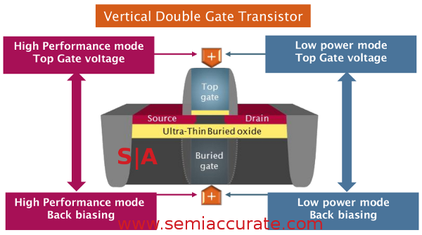
The idea is pretty simple in concept, take a FD-SOI wafer, and build your 28nm SoC on it. ST-Ericsson did just that, and developed a dual gate process that is actually quite a bit simpler than the ‘old way’ of doing 28nm on bulk waders. This new process was developed in their Crolles fab, but there is an agreement to port it to Globalfoundries on 28nm and 20nm. The process uses Soitec SmartCut wafers, and uses it to good effect. The FD-SOI layer means that ST_Ericsson doesn’t have to do any doping or strain to achieve the numbers they wanted, vastly simplifying the fabrication process.
A 28nm FD-SOI transistor
On the down side, FD-SOI wafers cost about 12% more than normal 28nm wafers, and have only one supplier. Balancing this out is a 15% reduction in process steps, the overwhelming majority of which are common with 28nm bulk processing. The net cost ends up being about the same for bulk and FD-SOI in 28nm due to the lower number of steps, but yields and performance are higher on FD-SOI. More for less at a higher speed, how can you complain?
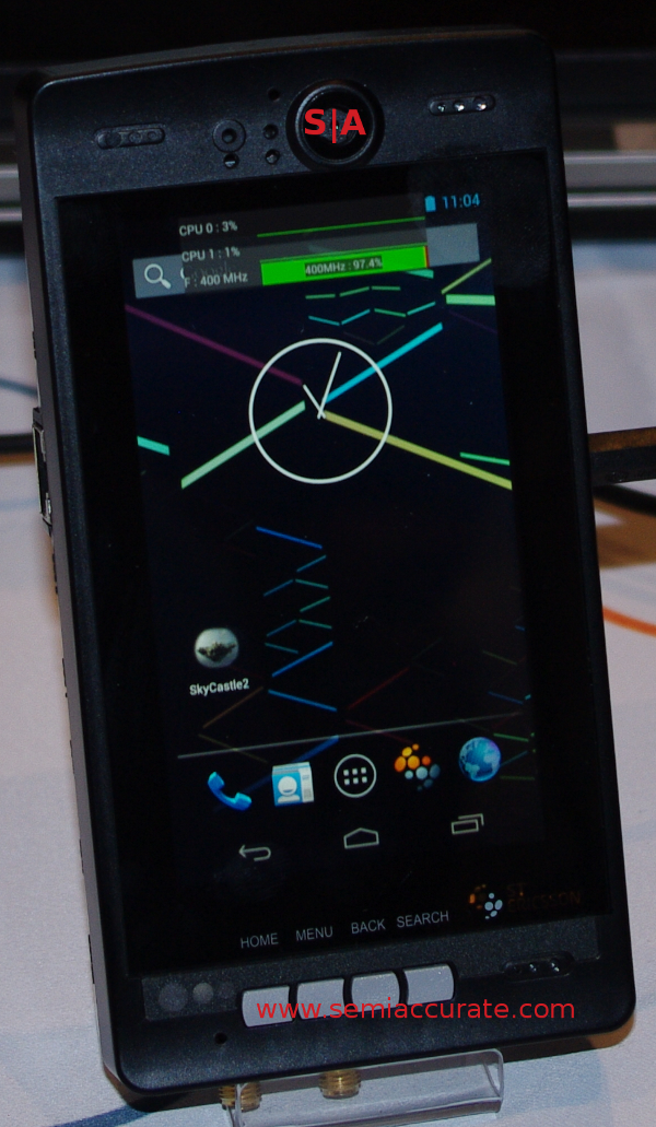
ST_Ericsson 2.5GHz Novathor L8580 development platform
The numbers for the new Novathor L8580 vs the older bulk L8540 are pretty astounding. Both share an identical layout, are software and pin compatible, and are basically equal in a functional sense. The old L8540 runs at 1.85GHz and had the fastest graphics of any ARM SoC when it came out in early 2012. The new one runs at 2.5GHz but uses the same power on paper, a bit less in the real world.
To give you an idea of how efficient this chip is, it will run at 1GHz on an astoundingly low .65V. Officially, ST_Ericsson is claiming 35% faster top speeds at the same power level, 25% power reduction at 1.85GHz, 50% power reduction at 800MHz, and 20% lower GPU power or 20% more performance at the same power level. The CPU cores are ‘only’ A9s, but a 2.5GHz A9 is a pretty formidable single threaded beast, and nothing comes close at the power levels we are talking about. These benefits also translate over into the LTE modem with a claimed 12% less power used in an LTE call.
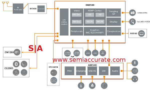
Novathor L8580 block diagram
In the end you have a full dual core A9, very solid graphics, and power consumption that no one out there can match at 1GHz. All this through a simple port from bulk to a novel FD-SOI process. No one was expecting this to come out, much less come out at CES. The best part is that while the demo rig above was running at 2.8GHz, more is promised in the near future. How many times can you say that the SoC that a company is releasing is ‘only’ being productised at 2.5GHz, is anyone else on the market at even 2GHz yet?S|A
Update 1/23/13 @ 4:10pm: You can hind the ST-Ericksson white paper on eQuad and 28nm FD-SOI here.
Charlie Demerjian
Latest posts by Charlie Demerjian (see all)
- Nuvia Founders Have A New Startup, Nuvacore - Apr 16, 2026
- Nvidia Is Negotiating To Buy A Large PC Oriented Company - Apr 13, 2026
- Dell Does Modular Laptop Boards Right - Apr 7, 2026
- Qualcomm Snapdragon X2 Review Embargo Lifts Tomorrow Morning - Apr 6, 2026
- Intel Cuts HDR OLED Panel Power with SmartHDR - Apr 2, 2026


