![]() SemiAccurate told you about ARM’s new M7 core last year, now we can go much deeper. Sit back, turn off that reality TV show, and enjoy lots of technical minutia about embedded CPU cores.
SemiAccurate told you about ARM’s new M7 core last year, now we can go much deeper. Sit back, turn off that reality TV show, and enjoy lots of technical minutia about embedded CPU cores.
If you are expecting something that rivals an A57 or A72 CPU, you are going to be disappointed by the M7, it is at the polar opposite end of the spectrum. For example the first M7 SoC out of the gate was the STMicro STM32 F7 line which is built on a 90nm embedded flash process and runs at 200MHz. Their roadmaps show that a 65nm device is up next and may run at a screaming 400MHz, silly fast for an embedded SoC but not even close to modern Cortex-A core clocks.
With that in mind, what’s the big deal? Efficiency mainly, that and servicing the rather unique needs of the embedded world which are often quite different from the mainstream CPU space. One good example of this is interrupt handling, ARM sacrificed a lot of performance to keep worst case interrupt latency low, a consumer CPU would never consider such things. Then again you probably would not put a consumer CPU in your critical medical device because most people want predictable latency there. There are a lot of tradeoffs that are made differently here, and all for a good reason.

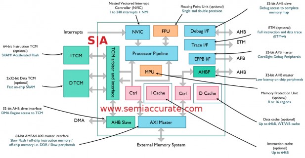
ARM M7 core block diagram
Looking at the block diagram, not much has changed since we first told you about the core but a few things were fleshed out. Starting in the top right corner we have the Debug and Trace interfaces. Debug has access to the complete memory map and is accessed as an AHB slave, useful but not game changing. Trace on the other hand has what ARM calls ETM or Embedded Trace Macrocell v4 which can access the full instruction stream. This is optional but given how important and likely small it is, why buy an M7 core without it? In short the M7 makes coding and debugging a lot easier.

ARM M7 pipeline diagram
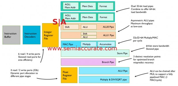
Things get interesting when you look at the pipeline in great detail, some things are a bit out of place. The first place to look is the Instruction Decoders, note plural. Looking back at the previous pipeline diagram here, the Issue block has “(2nd dec)” under. This is because some instructions are decoded early and others are decoded later for efficiency, or not decoded if there is no need. The M7 is a dual-issue machine and will do just that as long as there are two ops to issue. If the first decode can fill that, why spend the power decoding a second op. If the first one doesn’t fill, then the second one can.
If you look at the fine print on the Integer Register File, it says it has six read and four write ports, the FP Register File only has four read and two write ports. The interesting bit here however is the following part that says “Skewed read ports for area efficiency”. Look at that and also the ALU pipelines, note how ALU1 is skewed from ALU0. The point behind the ALU skewing is twofold but the result is a zero cycle latency generate-store penalty between pipelines. This means there is a zero penalty for Int or FP ops followed by a store or loads followed by a store.
The load-use penalty is also minimized by an early forwarding path in the load path. A load can place a result into the start of the pipeline that uses it rather than at the tail of the load pipe avoiding a 1 cycle bubble and boosting efficiency. Similarly there is no penalty for loads to ALU or shift operations but a load to AGU has a 1 cycle penalty. In short ARM did a lot of work to avoid penalties between many kinds of ops, skewing pipelines is not something you do lightly.
Skewing the second ALU pipe allows for an interesting optimization, you can issue two ALU ops with dependencies simultaneously avoiding some painful waits. Instead of waiting for a result then issuing the second ALU op, you can issue both and the skewing effectively delays the second long enough to obviate dependency problems. If you think about the compiler headaches and potential code bubbles this avoids, it is a worthy optimization.
One other thing to note is that there are two load pipes but only one store pipe even though the bandwidth for both loads and stores is the same. This is because the load pipes can each handle a 32-bit load while the store pipe can only handle a single 64-bit store. There are optimizations around this that we will discuss later on, this difference is intentional.

ARM M7 FP pipeline diagram
Moving on to the FP side of the core we see some similar tricks, specifically the skewing of the two pipes. The first FP pipe is ‘simple’ pipeline, the second handles more complex ops like multiply, divide, and square roots. Since they are skewed the generate-store penalty is minimized. Better yet you can chain the simple pipe to the complex pipe which means you can issue one FMAC per clock with zero pipe to pipe penalties. This is done via dynamic allocation of the second pipe and register pointers, quite a nifty hack. As an aside you can issue one MAC or FMAC per clock and these two instructions are the only ones on an M7 that can complete out of order, the rest are strictly in order. You will win money on that at a trivia contest some day, trust me.
The FP pipelines are all optimized for single precision but can do double precision with far greater efficiencies than software but not quite as good a s fully DP oriented pipeline. Given the workloads the M7 core is aimed at, there isn’t much heavy DP FP needed in the space. One other neat feature is that the FP pipeline can stall at any stage so DP FP and complex ops like subnormals are a lot easier to pull off with the limited resources of an M7 core.

ARM M7 front end diagram
Moving on to the front end we get to an interesting part of the M7 core, fetching and branch prediction. Possibly the most interesting part of the whole presentation were the compromises made here. When asked a few, “why didn’t you” type questions, the M7’s architect said that this part was a compromise. While branch predictions and fetch are critical to performance, getting that last few percent or fractions of a percent efficiency out of the unit takes a lot of area and power. Both of these things are items high on the list to minimize in any new design and ARM didn’t opt for the best possible theoretical solution in terms of hit rate.
Instead they went for the knee of the curve, a good predictor and fetcher that has minimal area and low energy use. In short it is good enough. That said the differences between the M7’s unit and a top of the line version is likely fractions of a percent, not even high single digit percentages. The result should be in line with the goals of the chip, highly efficient, low power use, and better than it’s predecessor.
Luckily for ARM there are several other optimizations that feed into the branch predictor and fetch unit that can ease it’s burden. First is that the M7 uses the Thumb2 ISA, not the newer ARM ISAs and so there are a lot of 16-bit instructions. That means the instruction fetch bandwidth is lower than on newer architectures and ISAs making things a bit easier. The fetch pipeline is also two stages plus one pre-decode stage that can be sort of counted here.
The AGU for fetching is 64-bits wide so you can pull in up to four instructions at once. This is handy for issue density and IPC but it has some potential problems especially for branches. The BTB has a 64-entry, 16-way branch predictor which coupled with the fetch width can mean multiple branches in a single fetch. On some architectures this can cause a lot of headaches but the M7 will handle that scenario. One thing that helps here is only caching 12 bits of offset data so a lot more branches can be stored in the area allocated for the BTB. The end result is more than enough accuracy and low energy use, couples with a zero cycle turn around.
Fetches cost, failed ones cost more, and if you don’t have to do either, you win. The longer a mispredict goes on, the more energy it costs plus the more flushing and waiting you have to do afterwards. It can be painful when things go wrong. In the execution pipeline there is a static predictor early on to detect BTB misses, this can occur as early as the first stage of the branch pipeline.
After that there is some early attempted taken/not taken resolution logic to pick off what the static predictor missed. This uses dedicated forwarding paths from earlier points in the pipeline. If all that fails there is a two stage resolution at the end of the branch pipe to hopefully minimize mispredict penalties. All of this both minimizes energy wasted and pushes up IPC for the M7, the more the better.
The final bits of the branch and fetch path are a fetch queue and instruction buffer. While they may sound complex, the fetch queue is mainly there to decouple fetch from execution. Similarly on the instruction buffer side but it also does some timing decoupling between fetch and execute. Together they buy a little more time and flexibility for the following stages so things can be optimized better.

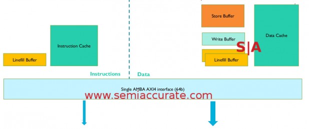
ARM M7 AXI bus memory diagram
Next is the big one, the memory subsystems, and there are two. First up we have the main memory system that is dominated by the AXI4 bus, a massive step up from the AHB buffers of older M-series CPUs. This bus is optimized for throughput and efficiency when coupled with slower, off-chip memories. This is the long way of saying it tries to hide latencies while maximizing bandwidth used.
Since the M7 doesn’t do any prefetching of data, you can use a lot simpler external memory. This directly translates into cheaper memory, a very good thing for the space the M7 plays in. One word of note, the M7 core is very configurable for different tasks so the caches, memory subsystems, and all the associated hardware may be very different or even absent between M7 implementations.
On the instruction side there is a linefill buffer and an Icache. The Icache is 2-way set associative and can be sized from 0-64K. It is a very simple system and quite unlike the data side of the chip. The Dcache is 4-way set associative and can run from 0-64K just like the Icache. It also has limited support for dual-issue loads even to different lines. The limited caveat means the M7 can get away with only using single ported memories saving costs, it is another tradeoff.
There is also another linefill buffer, a store buffer, and a write buffer on the data side. The store buffer can hold four 64b entries for heuristic draining, basically keeping things in storage as long as possible in the hopes of merging stores. This saves bandwidth and more importantly energy. The buffer can be configured for write through or write back depending on the needs of the implementor. Data linefill buffers, there are two, support dual independent loads.
On the bus side the instruction fetch can have one ID and one outstanding transaction, it isn’t that complex. The data side can have three IDs and six outstanding transactions on the read side, four IDs and 39 outstanding on the write side. As you can see the data side of the AXI memory subsystem is significantly more complex than the instruction side.

ARM M7 TCM memory diagram
ARM’s M7 has a second completely different memory subsystem called the TCM or Tightly Coupled Memory subsystem. This is one way that the M7 can meet its strict interrupt latency goals, a must of embedded cores. The TCM is hung directly off the CPU and is both simple and fast, almost exactly the opposite of the AXI memory. TCM memories are also on-chip for speed and power use but don’t think of it as a cache, it is memory.
The closest parallel to the TCM interface is SSRAM and it supports wait-states, errors, and byte-writes. All of the memories on the TCM sit on a crossbar with QoS capabilities to arbitrate between core and DMA requests.
There are three possible memory blocks on the TCM, the ITCM and two DTCMs. The ITCM is 64-bits wide to line up with the instruction fetches and the DTCMs are 32-bits wide each to line up with data fetches. The data addresses are banked based on bit 2 of the address so you can hit them both independently which aligns with the core’s data load capabilities. TCM memories can be sized up to 16MB, not a lot but huge for embedded.
There are five total connections to the TCM crossbar which are not memory. Three of these, the 64-bit wide instruction fetch and the two 32-bit data fetch ports are quite obvious. The other two, a store queue and a DMA slave port aren’t nearly as obvious. The store queue is just what it sounds like, a small buffer optimized for the memory types the TCM will use. This saves power and memory cost but doesn’t do any fancy tricks, it is a just simple queue. The DMA slave port is mainly there for older AHB bus devices that need to access TCM, handy if you have older IP blocks to bring into the M7 world.
You might have noticed that we mentioned interrupt latency several times in various places and there was a reason for that, it is one of the main design goals of the M7 core. You could say that the core was designed to minimize interrupt latency because, well, it was. Instead of using software to handle a lot of interrupt work, the M7 puts as much of that in hardware as possible. The net result is an 11-12 cycle interrupt latency, quite low for such a complex and critical task.
One of the things now done is hardware are fetching and branching to the specific interrupt handler requested, this can shave quite a few cycles off the top. There are also eight Int registers stacked so an interrupt can start work without delay. On the FP side there is lazy stacking of 16 FP registers, stacking is handled only if the interrupt uses FP. All of this is included in that 11-12 cycle count, that is a real world number that includes everything.
There is also a direct, high performance path from the interrupt controller to the pipeline for efficient interrupt processing. The instruction queue also supports bubble closing, it can start a decode of an interrupt instruction even if the pipelines are stalled at the time of request. The rest of the pipeline is designed to ‘aggressively’ flush if an interrupt is asserted, no need to make a cheap joke on that one is there? An interrupt can also kill one of the issue slots without killing the other, handy when resuming and saves a bit of power too.
Since the core is mostly in-order on the completion side, most of the hazards created by an interrupt induced stall simply aren’t there. This simplifies things quite a bit. On the memory side there are several useful functions that aren’t allowed because they would cause problems for interrupts. One of these is bursts for volatile load/stores of multiple registers, they are just not allowed. Normal memory bursts can play nicely with interrupts so they are allowed. Similarly load/store issue pairs are serialized so an interrupt doesn’t have to wait if issued in the middle. In short there are a lot of things that would be useful to have on the M7 but are not allowed because of the effects on interrupts. This coupled with the hardware handling of tasks previously done by software allow for relatively high clocks, high performance, and still keep interrupt latencies very low. This is not a big deal in the PC space but deadly important in embedded.
In the end you have a painfully simple CPU by PC standards but a monster compared to embedded cores. Compared to the older M4 core which it is software compatible with, the M7 is somewhere between 1.5-2x faster on the same code. Some of this comes from architecture, some from higher clocks, and some from better memory and caches. Lets just say it is much faster and more efficient when doing the same work and also has much more headroom. The only downside is that the M7 core is much bigger than the M4, more than 2x. On TSMC’s 40LP process at a 200MHz target clock, the M4 takes .1mm^2 of space while the M7 hogs .23mm^2. If that doesn’t illustrate the difference between the PC and embedded worlds, nothing will.S|A
Charlie Demerjian
Latest posts by Charlie Demerjian (see all)
- Nuvia Founders Have A New Startup, Nuvacore - Apr 16, 2026
- Nvidia Is Negotiating To Buy A Large PC Oriented Company - Apr 13, 2026
- Dell Does Modular Laptop Boards Right - Apr 7, 2026
- Qualcomm Snapdragon X2 Review Embargo Lifts Tomorrow Morning - Apr 6, 2026
- Intel Cuts HDR OLED Panel Power with SmartHDR - Apr 2, 2026