 AMD just launched their mobile new APU called Carrizo today, lets take a look at it. SemiAccurate was briefed a little while ago so let’s go in to the architecture as deeply as we can.
There are two main parts of Carrizo, the CPU and GPU, both of which are fairly well-known quantities at this point. The CPU is the first public appearance of the Excavator core while the GPUs are the familiar Volcanic Islands/VI generation. All of this is tied together by an HSA1.0 compatible fabric. Since Carrizo is a mobile part it is specced at a 15/35W TDP for actual technical reasons we will explain later. As is normal in new chip launches, the interesting stuff is not at a high level, it is all about details.
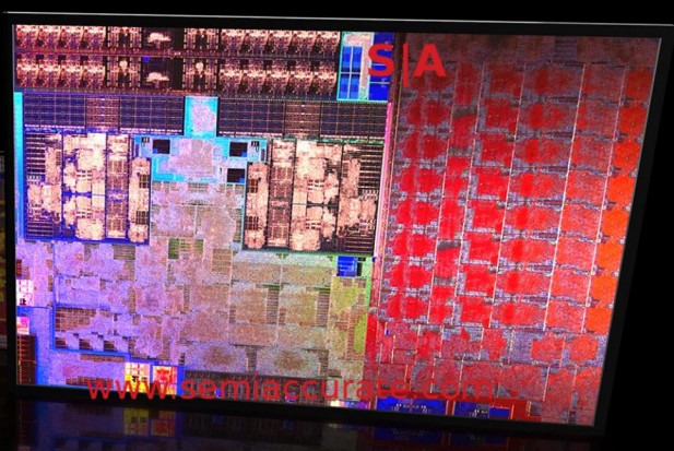
It kinds looks like this unskewed
Everything starts out with a pair of excavator modules also known as four CPU cores. Excavator is a known quantity with much of the core being disclosed at ISSCC last year. As has been the case since Bulldozer, cores are paired into a module with each successive generation slowly peeling apart the shared features. At the moment the Excavator core is effectively two cores with a shared FPU. While this approach has some good sides and some bad, it is the only way you can get an excavator core.
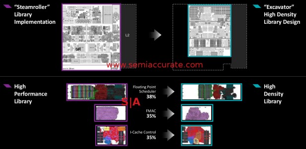
High density libraries are just that, see?
More important than the core itself is how it is built, it is designed with non-CPU oriented high density libraries normally used in GPUs. This approach reduces area so Carizzo is actually fractionally larger than its immediate predecessor Kaveri. Carrizo weighs in at 250mm^2 vs Kaveri’s 245mm^2, a bit of an increase but Carrizo integrates the chipset which Kaveri had on another die. AMD is claiming a 23% decrease in area for the core itself and some blocks are significantly smaller than that. Both are built on the same 28nm process.
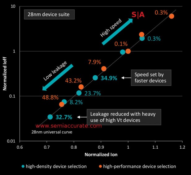
Note the percentages
The down side of this change is interesting too, on a normal ‘high performance’ library you get a bell curve of GPU yields with a large number of low-speed parts and a few high performance versions. With ‘high density’ libraries you get a much different curve with the bulk of the parts sitting in the middle bin and the curve being flattened quite a bit. The absolute peaks are lower too as you might expect from the library names. In short there are more mid-range bins that sell in volume and less halo parts that don’t yield enough for a realistic marketable SKU. Not a bad trade for such a large area savings.
Moving back to the details, there are a few new bits to talk about. Things start out with a 512KB L2 cache, then move on to a doubled L1I cache, it is now 64KB. L1D is unchanged at 32KB, and latencies for both are the same as Kaveri. In case you are wondering, the L1I is 8-way and the L1D is still 4-way. As a power savings trick, AMD segmented the word lines so non-needed data is not read which saves quite a bit of power.
Backing this is a much larger BTB, 768 entry vs 512 on Kaveri which should help in branchy code. AVX2 is now supported as is the AES-NI instruction set. AMD claims there are also “modern standby low power modes”, about time. All of this means AMD is caught up on the ISA front and getting closer as far as power modes are concerned.
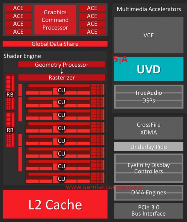
This GPU should look familiar
Moving on to the GPU front things are a bit less interesting. The shaders are VI generation with 8-cores aka 512 shaders backed by eight ACEs for compute and HSA functions. At a high level, the GPU isn’t very interesting mainly because the architecture has been released as a discrete part years ago. There are a lot of details and additions on the video front that are worth talking about though.
The biggest of these additions is the new UVD 6 block which brings hardware H.265 decompression and 4K H.264 support. As you might expect AMD has upped the bandwidth to the UVD block by 4x to support the 4x higher pixel throughput. Since most people don’t use 4K video yet, this translates to large power savings at 1080p resolutions, if you can sleep the GPU for 3/4 of the time you can save tons of energy.
Another trick is the block labeled “underlay pipe”, effectively a scaler and image processor in the display controller. Traditionally the output from UVD was stored out to memory, read back to the GPU for processing, written back to memory, read by the display controller, and then output. Memory writes are slow and power intensive so you want to avoid them whenever possible. The underlay pipe effectively adds the functions done by the GPU to the display pipe so a full round trip to memory is removed and the scaling is done in dedicated hardware. This saves a lot of power.
Carrying on this power savings scheme is memory compression, common in the cell phone world but just starting to creep into the PC space. AMD claims this will save 5-7% of memory reads and writes effectively increasing bandwidth and saving power by about the same margins. The compression is lossless so it there really isn’t a down side to it.
AMD is now officially admitting there is an ARM Cortex-A5 on their APUs, something we told you about years ago. It is part of a block called the PSP and since it is ARM based, it means you can implement Trustzone on the AMD APUs now. It may not sound like a big deal but it very likely drops certification and testing time by large amounts which also saves quite a bit of money. Implementing an accepted and ‘known secure’ product is much smarter than rolling your own.
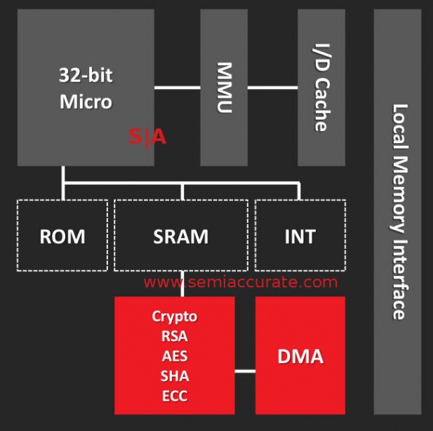
This is how security is done, vaguely
From the bullet point side of things the PSP hits the key features but as usual it is the implementation that makes or breaks a device. There is on-block ROM and SRAMs for secure storage and calculations plus a OTP for device unique keys, both basic requirements for security. Adjacent to this is the control logic for x86 boot so that side should be ‘secure’ or at least much harder to spoof. Last up there is a crypto co-processor that can do the usual tricks, RSA, SHA, ECC, EAS, ZLib, and TRAND (hardware random number generator). The PSP can DMA things to the main system, again about what you would expect.
Stepping back a bit we have the bus between the main units, in this case it is Onion3. You might recall that in days of yore there were two busses, Onion and Garlic. With the further integration of functions in Carrizo there isn’t a need for two busses anymore, Onion3 combines the functions of both into a simpler layout.
What this means is that Carrizo is now fully HSA1.0 compatible so you can do all the tricks laid out years ago, we are finally there. The main new addition is GPU preemption, it is now a full citizen of the compute world, not just for graphics anymore. This also includes coherence, context switching, preemption on 3D workloads, QoS, and snooping. If you are wondering why GPU compute can fully context switch while graphics is stuck with preemption, it is a resource issue. Compute needs far less to switch and graphics doesn’t really make sense to swap like that, just let the pipe flush out and call it done. The GPU now has full access to the memory controller with all the advantages that brings, the eight ACEs can almost be considered CPU cores now.
For outputs Carrizo can support three outputs and all three outs are full DP1.2 ports. Backing this up are 4x USB3 plus 8x USB2. There are eight PCIe3 lanes if you want to add a GPU, something Oxide was showing off the power of with a Mantle version of Ashes of Singularity. It handed off compute task between a Carrizo and a 290 seamlessly, assets on a single frame could come from either place.
Last up we come to power, both on die and as a product. Carrizo has three power rails, GPU, CPU, and NorthBridge. This allows for optimization and the usual power gating features, plus optimizations for the particular frequency ranges each component lives at. That however doesn’t explain the 15/35W TDP ranges for the given SKUs, and that is a bit of a long story.
The shortest version is that base clocks have become almost meaningless lately, things can turbo up and down on such a granular scale that base clocks are almost a curious anachronism. If you are not using blocks at their top available frequency, you are wasting energy. If they are not being utilized, is there a point to keeping them awake? If you can swap clock ranges on a tens of cycle basis, how long do you think a device will be resident at an arbitrary frequency listed on the store shelf? That said it is still nice to know the number.
Moving back to Carrizo, what is the TDP? The devices are optimized for a 15W TDP level but they will go up to 35W if needed. Normally you take a part and bin it on the top rated speed it can go, then secondarily on power. This time around AMD doesn’t differentiate on TDP levels they take a fixed TDP, in this case 35W and see what the parts can run at while staying under that cap. So instead of being binned on peak frequency, Carrizo is binned on peak power use.
This allows AMD to do something interesting, since the parts are optimized for a fixed wattage, they are all shipped as 35W parts. An OEM can then set the peak TDP based on the thermals of the design in question, if it is thin and light, 15W, big and heavy, 35W. This only takes a BIOS or firmware change, the underlying silicon is still the same.
The end result is that the wattage of Carrizo ends up not determining peak frequency, it is the same regardless of the setting, but how long the part can be resident at that frequency. If a theoretical Carrizo is specced for 2.0GHz CPU and can sit at that frequency all day at 35W, cutting it down to 30W may mean it can only sit there for 95% of the time. As you lower the TDP setting, turboing to the top bin comes more infrequently. In short the peak turbo is the same, how often and how long a device sits there is what the wattage slider controls.
In the end there is only one question, how well does Carrizo perform. When we said question we actually meant it though, that wasn’t a rhetorical statement, we don’t have a clue how well it does. AMD did not supply test systems this time around because some reviewers didn’t feel that a demo system was representative of real world devices so we have to wait for those to come out.
While these should be on the market in the very near future and Computex is full of pretty good-looking Carrizo devices, until they do we have no idea how it will perform. When they do we will let you know how well the claims stack up to the real laptops but we won’t reprint the claims blindly. It should be much better than Kaveri but exactly how much and at what is still a mystery. Lets hope OEMs release the designs soon, I can’t wait to play with them.S|A
Charlie Demerjian
Latest posts by Charlie Demerjian (see all)
- Nuvia Founders Have A New Startup, Nuvacore - Apr 16, 2026
- Nvidia Is Negotiating To Buy A Large PC Oriented Company - Apr 13, 2026
- Dell Does Modular Laptop Boards Right - Apr 7, 2026
- Qualcomm Snapdragon X2 Review Embargo Lifts Tomorrow Morning - Apr 6, 2026
- Intel Cuts HDR OLED Panel Power with SmartHDR - Apr 2, 2026