![]() ARM is adding the new CMN-600 and DMC-620 to get a first for them, a backplane. SemiAccurate thinks this new interconnect and memory controller add up to a real sea change for the ARM world.
ARM is adding the new CMN-600 and DMC-620 to get a first for them, a backplane. SemiAccurate thinks this new interconnect and memory controller add up to a real sea change for the ARM world.
Fool us once, shame on us, fool us twice shame on us again, fool us three times and we get annoyed. Luckily we only took the CCN- numbering bait once when we opined that the follow on to ARM’s 32-core CCN-508 interconnect would be the CCN-516. It was the CCN-512 and after that we stopped speculating. Luckily that was the correct path because the CCN-‘s replacement is not a Cache Coherent Network anymore, it is the CMN-600 or Coherent Mesh Network. Not only is this new interconnect between 88 and 98 better, it is ground up radically different.
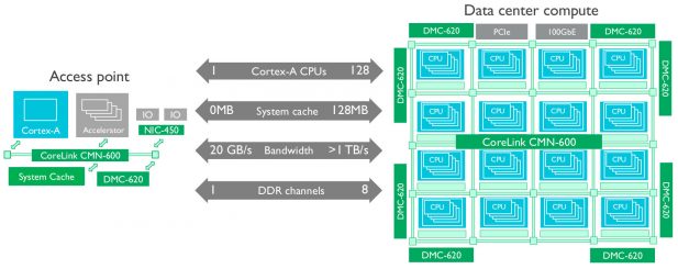
Scales small to large
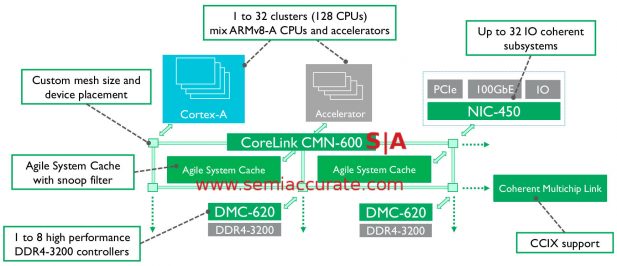
For starters it is a mesh not a ring and supports far more CPU cores than CCN-512 ever could. Each node can support two arbitrary blocks be they CPU, cache, or something else entirely. The numbers you see above probably have a bit more flexibility than ARM is admitting to at the moment, time will tell. That said you can officially have up to 128 cores or 32 clusters of four as is the ARM way, 128MB of “agile system cache”, and eight DMC-620 memory controllers all on one SoC.
CMN-600 node details
As you can see the clusters above can be either ARM v8-A CPUs or accelerators plus 32 coherent I/O devices. Since the CMN-600 line has a practical but not architectural limit of 8*8 nodes, this 32 cluster or I/O limit seems to be architectural for now. The presence of a CCIX link on the edge alludes to the hardness of the core count though, we expect at least a few designs to push some interesting numbers in the coming years when CCIX is fully fleshed out. That said the DMC-620 supports up to DDR4-3200 memory plus has support for HMB-like stacked RAM so the SoC should be well within reasonable bandwidth limits up to pretty high core counts.
Speaking of bandwidth, each link between nodes is 256b wide and can run up to 2.5GHz or 640Gbps per link, ARM officially claims “>1TB/s” bandwidth for a system, something we can believe will be achievable. If you have an 8*8 mesh, the cross-sectional bandwidth would be 2Tbps which is still a pretty impressive number. We didn’t ask if it was unidirectional or bidirectional, we suspect it is bidirectional so you can probably double that number safely.
ARM officially said that “if 10 cores are each requesting 100GBps, they will get it”. We look forward to more in-depth routing details, there is probably a lot of neat tricks lurking if that claim is true. The mesh can dynamically scale frequency as is the current norm but as always, that is optional if you have a use case that doesn’t play well with potential jitter.
That brings us to the cache or agile system cache in newspeak. It can be placed around the mesh rather arbitrarily but there are probably size and count limits. About all we can say specifically here is the total limit is 128MB or 1MB/core when a CMN-600 mesh is fully kitted out. The interesting bit is why ARM used the word agile in their naming, it isn’t just for show.
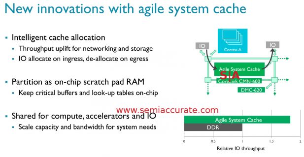
Cache is not as dumb as it was anymore
The first point above is Intelligent Cache Allocation, a chunk of a cache can be blocked off and allocated to a use on demand. While this can be done at boot, it is flexible even on a running system for things like networking and I/O to use as their own private caches or packet assembly/disassembly areas. The allocation here is done at a driver level or below, it is not a userspace visible feature for obvious reasons. To give a good example of the flexibility, the cache can be read and de-allocated with one command to not waste space. If there are no lurking gotchas here, it looks to be a very impressive feature.
For more long-term use cases the second bullet point of on-chip scratch RAM is more applicable. This mode is more of a subset of the flexible allocation above but it is still worthy of pointing out especially given the throughput graph above. Roughly double the throughput is nice but a lot of the tasks ARM lists are very latency sensitive and that graph would be far more lopsided that the throughput one. In short ARM allows a system designer to pull off some nifty and extremely useful tricks with the agile system cache and we can’t say we have heard of anything else that comes close to this functionality.
With this flexibility on the cores, cache, and placement, we had to ask about hard partitioning. In a surprise to no one the CMN-600 supports partitioning of resources at many levels. The obvious hypervisor based partitioning is there but many users, *COUGH* telcos *COUGH* who we won’t mention usually require more than that. Luckily for them the CMN-600 can do at least two hardware level partitions ending up with a NUMA-on-SoC device or something like that.
Officially ARM lists four differences between the CCN + DMC-520 line and the CMN-600 + DMC-620 lines. Those are working groups for application isolation, end-to-end data path parity protection, new RAS logging and reporting architecture, and support for 3D stacked memory. While these are all nice, they don’t mention the fundamental change from rings to meshes nor the massive flexibility of the cache allocation features. You have to wonder what other goodies aren’t publicly disclosed yet.
On a related note ARM is promising some equally impressive updates to their tool set for making devices with the CMN-600 and DMC-620. All this flexibility and complexity obviously demands an exponentially greater validation program and ARM is addressing that with CoreLink Creator and the Socrates Design Environment. They promise automated placement, replacement, and the like with RTL generation in “minutes” if you use CoreLink plus automated connectivity with Socrates. If ARM can automate the hard part of a massive mesh system, licensees will be more than a bit happy.
As you would expect from licensed IP, ARM has validated the underlying blocks to their usual degree, possibly more if the target market is large multi-core servers. To speed up the validation of the resultant designs, you need to run validation tests until you get bored, turn blue, die of old age, and then as much more as you can. To help this ARM is offering FVP or Fixed Virtual Platforms. As the name suggests this is a virtual testbed environment with open source drivers and Linux OSes to test your potential design on. It may sound simple but it takes a lot of the hard work out of system prototyping and design, you don’t have to do the annoying OS bringup work on your own, for ARM IP it now comes pre-packaged.
In the end we have a potentially game changing set of designs that can be made using ARM’s new CMN-600 mesh interconnect and DMC-620 memory controller. Even if you run without DMC (come on, I had to do that pun somewhere), it is optional, this new interconnect will allow for ‘real’ large systems using ARM cores. Officially the sweet spot for DMC-600 will be 64-cores on a 7nm process but the fun comes in with the flexibility. I can’t wait for the first few system disclosures using this backplane, it could do for servers what ARM’s IP did for mobile devices.S|A
Charlie Demerjian
Latest posts by Charlie Demerjian (see all)
- What is Qualcomm’s Purwa/X Pro SoC? - Apr 19, 2024
- Intel Announces their NXE: 5000 High NA EUV Tool - Apr 18, 2024
- AMD outs MI300 plans… sort of - Apr 11, 2024
- Qualcomm is planning a lot of Nuvia/X-Elite announcements - Mar 25, 2024
- Why is there an Altera FPGA on QTS Birch Stream boards? - Mar 12, 2024