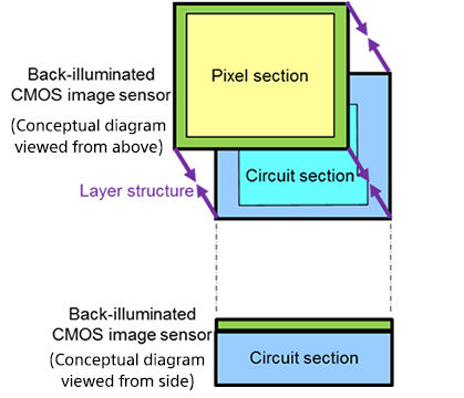
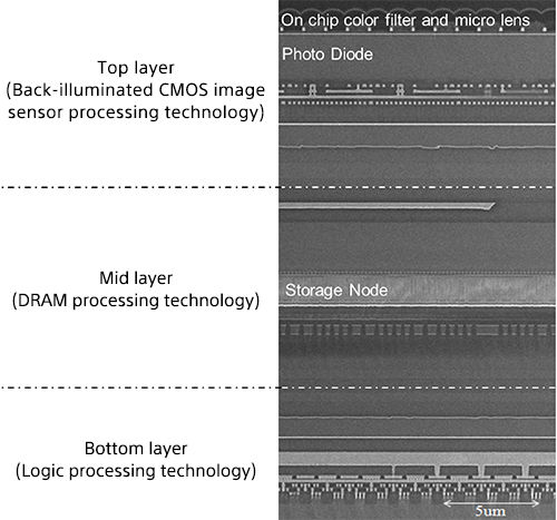
In a briefing at ISSCC Sony announced the creation of the first three-layer stacked image sensor. This design takes a DRAM die and sandwiches it between Sony’s well know BSI image sensor and the support circuitry necessary to read out the image sensor. This is an interesting solution that differs from prior 3D stacking design where the stack is usually composed of a homogeneous set of dies like in the case of an HBM2 stack. Existing designs like GP100 and Fiji have used a 2.5D stack that includes a large interposer to facilitate communication between ASICs and stacked memory. Sony’s solution does away with the interposer entirely when stacking dies with different functions like image sensors, memory, and their support circuits.

The practical advantage to stacking a chunk of DRAM under an image sensor is that the pixel values can be cached in the DRAM before being written to longer term storage. This helps Sony address one of the biggest problems with modern image sensors: rolling shutter. Also known as the “Jello effect” rolling shutter is a visual artifact that occurs when there is movement in the scene that the sensor is capturing that is happening faster than the image sensor can read out all of its pixels.
Caching the Sensor Readout in DRAM
Thanks to the DRAM in this stack the image sensor can now be read out at a rate of 120 times per second. This means that for still images and 30 FPS video a smaller slice of time can be captured which will help significantly in reducing the appearance of rolling shutter. It also enables slow motion video capture at up to 120 FPS. According to Sony, the DRAM buffer enables read rates that are about four times faster than conventional pixel reading methods.
Given that Sony’s implemented this technology on a 1/2.3″ sensor it’s clear that they are aiming at this fast sensor readout capability at smartphones where, largely thanks to the iPhone, slow motion video capture is all the rage at the moment. In test footage, Sony demos sports and actions scenes that are recorded with this sensor at up 960 FPS capture rates. Of course, these extreme frame rates aren’t full sensor readouts rather they are lower quality crops. But still, it’s great to see that there is enough sensor readout bandwidth to enable this kind of image capture.
For this specific development product, Sony used only 1 Gbit of DRAM to enable these read rates. Obviously, if the company wanted to scale this technology up to APS-C and 35mm-sized sensors they’d have a lot more physical area to add additional DRAM capacity with.
Bringing Stacked DRAM to Market
Given that the first stacked image sensor for 35mm cameras rolled out in 2015 after Sony announced its development in 2012; we’ve probably got a few more years before this kind of fast sensor readout technology makes its way into DSLR styled cameras. But it seems clear that Sony wants to push its new sensors into phones as quickly as possible and given the competitiveness of that market I have no doubt that we’ll see products equipped with something similar to this stack in the next year.S|A
Thomas Ryan
Latest posts by Thomas Ryan (see all)
- Intel’s Core i7-8700K: A Review - Oct 5, 2017
- Raijintek’s Thetis Window: A Case Review - Sep 28, 2017
- Intel’s Core i9-7980XE: A Review - Sep 25, 2017
- AMD’s Ryzen Pro and Ryzen Threadripper 1900X Come to Market - Aug 31, 2017
- Intel’s Core i9-7900X: A Review - Aug 24, 2017
