![]() Qualcomm’s Snapdragon 845 continues a trend for the company, integration of the parts. As SemiAccurate has been saying for a while now, pure CPUs don’t matter much any more, the rest does.
Qualcomm’s Snapdragon 845 continues a trend for the company, integration of the parts. As SemiAccurate has been saying for a while now, pure CPUs don’t matter much any more, the rest does.
Qualcomm’s new Snapdragon 845 does start off with two new CPU cores which they collectively call Kryo 385. There are eight cores in total, 4x modified ARM A75s and 4x modified ARM A55s, neither of which had a distinct name called out. Qualcomm claims the big cores will top out at 2.8GHz and are good for 25-30% higher performance, something SemiAccurate saw in testing. Similarly the small cores run up to 1.8GHz and are a claimed 15% better than their 835 predecessors.
This is important because not much comes from the new process, Samsung’s 10LPP. For the process geeks out there the 835 was built on 10LPE, the E stands for Early, the last P in LPP stands for production. In any case not much more than a small bit of that performance uplift comes from the process change, think of it as a minor PDK update more than a new process.
The cores are arranged in a classic big/little array but the new ARM Dynamiq architecture allows them all to be in a single cluster. For caching all cores have a 64K L1D and 64K L1I cache but the big cores get a 256K L2 while the small ones only get 128K each. Even with these changes and the added features below, the Snapdragon 845 fits in the same 12.4×12.4mm package as the 835. It is a larger die but the package is still big enough to handle it although the two are not pin compatible. This is likely due to memory package sizes constraining the base of the PoP assembly.

The package in question on a questionable card
More importantly are the two changes Qualcomm listed for the cores themselves. As we mentioned earlier, ARM makes these customizations themselves and gives the core to Qualcomm. Both changes, bus QoS and page table security bits, are meant to work better with the uncore of the SoC. The bus QoS is just what it sounds like and is mostly controlled through a separate on-die controller that picks up what the SoC is doing and adjusts priorities for the workload at hand. There is some talk about exposing this QoS system to users and OEMs but for the moment it looks like that isn’t an option even if it may be in the future.
More interesting is the second major mod to the A75/A55 cores, pagetable addons for security. Lets start this out by saying that this isn’t for the system MMU’s page tables, it is for the page tables on the CPU itself. Qualcomm added in a few bits to enhance security although they didn’t get into details for obvious reasons. That said it is likely these bits are there to allow more states than the standard ARM Trustzone allows when working with the Secure Processing Unit, an external hardware security processor.
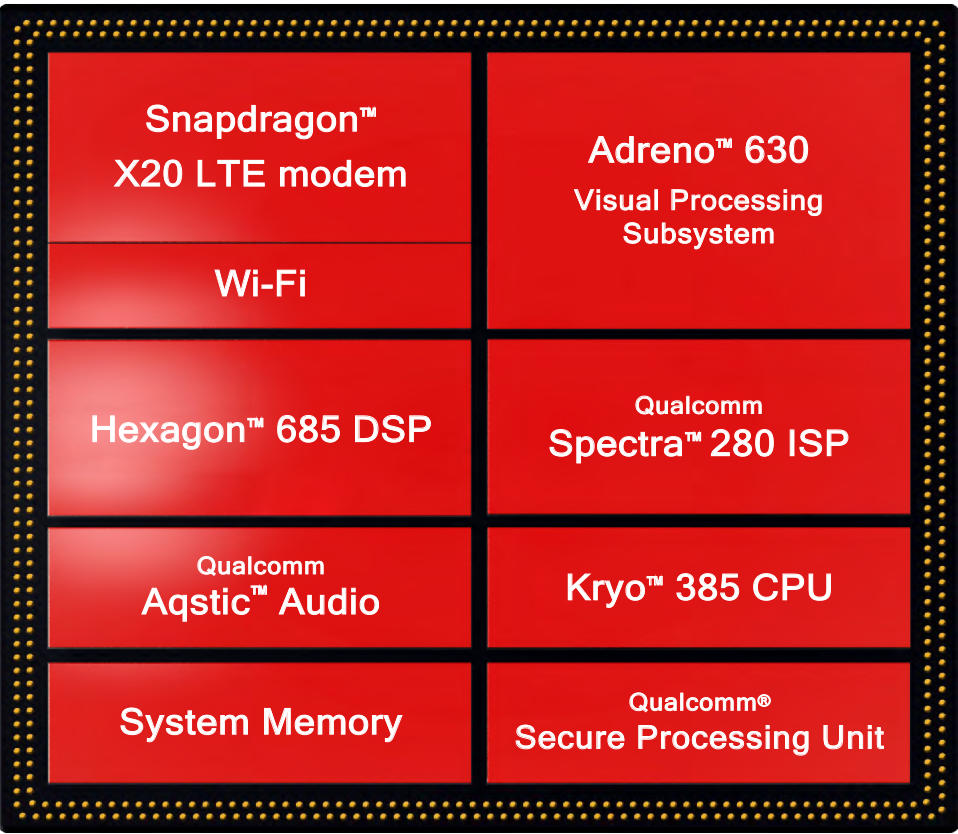
Snapdragon 845 blocky block diagram
The next big bang in the system is the Adreno 630 Visual Processing Subsystem aka the GPU. Like always Qualcomm is not giving out any useful architecture details on their GPUs, only vague performance numbers. Luckily those performance numbers appear to be good and do stack up in testing on early 845 reference designs. Qualcomm is claiming 30% better performance AND, not OR, 30% better power usage. On top of this there is a claimed 2.5x “faster display throughput” aka latency.
How did they do this? Without details we can’t know for sure but one thing that was said is the entire GPU was ripped up and replaced between the 835 and 845 generations. This isn’t to say the architecture was changed radically, just a redo for for efficiency and lower latency. One way this is accomplished is by much greater granularity for preemption, something that was also claimed for the Spectra 280 ISP a few months back.
The Adreno 630 can preempt on a primitive or workgroup boundary basis which is both fine grained enough and adds to efficiency. A task doesn’t have to wait for lots of geometry to be processed before it can push the results to shading, texturing, and other functions. This is also useful for foveated rendering which the 630 can do on a tile basis if there is good enough eye tracking. Multiview rendering is also included to drop latency and GPU loads. The left eye is rendered first, duplicated for the right, then ‘enhanced’ with changes for stereo vision. This saves tons of calculations and thus energy while vastly improving frame rates.
We mentioned most of the goodies in the new Spectra 280 ISP a few months ago but there are a few new ones. On the top of that list is full UltraHD Premium 4K capture at 60FPS, and yes we know the HD nomenclature is getting as silly as LTE but we can’t change that. What this brings to the table is 10b color, Rec.2020 color gamuts, luminance control, and per-frame metadata. Basically the 280 allows full use of the things HDMI 2.1 cables pass.
On top of that the Spectra now can process slow motion video, 720p480 to be specific. There was a bit of confusion about how fast it can do 1080p but simple math says 120FPS should be pretty easy, likely faster since 4K60 is possible. In the cute tricks category there is also now a mode for real time cinemagraphs, basically a still image with a subsection that moves. I dread the UI for this one, but it is a feature. The new ISP can officially handle up to seven cameras now should you need to do so.
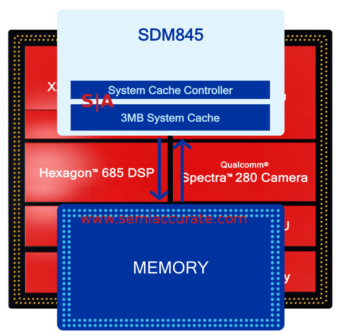
A really bad description of cache hierarchies
All of these new CPU and GPU features are nice to have but more features rarely make things faster or more energy efficient. Since both of those are key requirements for any new SoC, Qualcomm added a massive system cache to speed things up and lower energy use. There is now a 3MB system cache to feed the beast, it sits between the functional units and the MMU so it is not a pure memory cache. Qualcomm calls this the SDM845 and it has both memory and a cache controller. In practice it is good for a claimed drop in external memory use of 40-75% and a lot of power savings given the energy cost of an external DRAM access.
If that sounds like a lot to have in an SoC, the above is only half of the units found in the Snapdragon 845. We haven’t even touched on the DSP, audio, security, and modems yet. The good news is that they all have some pretty cool new features to add to the mix, especially on the security side. The bad news is that they are all for another day, stay tuned.S|A
Charlie Demerjian
Latest posts by Charlie Demerjian (see all)
- AMD outs MI300 plans… sort of - Apr 11, 2024
- Qualcomm is planning a lot of Nuvia/X-Elite announcements - Mar 25, 2024
- Why is there an Altera FPGA on QTS Birch Stream boards? - Mar 12, 2024
- Doogee (Almost) makes the phone we always wanted - Mar 11, 2024
- Intel Birch Stream Boards Speak From The SIde - Mar 6, 2024