![]() Intel gave a bit more away about their 20A process at Innovation, specifically a crucial detail about PowerVia. SemiAccurate noticed something in the slides and confirmed our speculation a bit later on.
Intel gave a bit more away about their 20A process at Innovation, specifically a crucial detail about PowerVia. SemiAccurate noticed something in the slides and confirmed our speculation a bit later on.
The idea is pretty simple, Intel’s 20A process, also known as 5nm in sane-speak, has two main advances, ribbonFETs and PowerVia. RibbonFETs are cool but if you think about it, while most foundries use FinFETs, Intel uses tri-gate transistors. Until Intel reveals a lot more about 20A and RibbonFETs, going from three to four sides covered by gates isn’t going to excite us all that much even if it is technically difficult.
PowerVia on the other hand is a lot more impressive. It is back side power delivery which means the big metal traces in the top layers of the die for power distribution and the vias bringing it to the transistors, are on the back of the wafer. This means power can be delivered much more directly to the things that need it and the routing of the lower metal layers can be vastly simplified by not having to go around those huge downward power delivery lines. It is a win/win if you can pull of the engineering even if you need TSVs to get it done.
One last thing about this tech, heat. If you put the transistors in the middle layers of the chip, the chip itself adds to the insulation making it harder to cool the sensitive bits. This is not new nor is it unique to Intel’s tech, it is effectively why we can’t do high power die in 3D stacks at the moment. One possible up side to the tech is that with flip-chip mounting, those big metal pipes directly from the transistors to the (now) top will wick out heat fairly effectively if used properly. Time will tell how this one plays out too, but back to the main story.
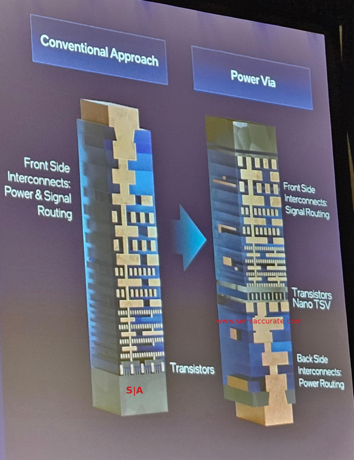
Innovation 2023 process talk slide on PowerVia
As you can see on the left, the ‘old way’ has the metal power distribution layers on top, PowerVia on the right has it under the transistors. The lessened routing complexity is not immediately obvious in the diagram but a new set of complexities arises with how you get those power traces to the transistors. Is it the same issue with TSVs where you have (relatively) massive holes with extensive keep-out areas or is it something more elegant? Time and hopefully more disclosure will tell.
That said there is one big clue in the pictures, did you spot it?
Note: The following is for professional and student level subscribers.
Disclosures: Charlie Demerjian and Stone Arch Networking Services, Inc. have no consulting relationships, investment relationships, or hold any investment positions with any of the companies mentioned in this report.
Charlie Demerjian
Latest posts by Charlie Demerjian (see all)
- Intel Bumps Xeon Memory Speeds - Jul 20, 2026
- Qualcomm’s 2026 Investor Day Has Hidden Goodies - Jul 15, 2026
- Phison Phudges The Numbers… In A Good Way - Jun 24, 2026
- Who Are The Qualcomm Enterprise Customers? - Jun 23, 2026
- Innodisk Adds 10GbE To Useless M.2 Slots - Jun 19, 2026