![]() Intel’s Clearwater Forest CPU line has a rather unique feature, it is mounted to two PCBs. Semiaccurate wondered why Intel used two substrates for this part and got a simple answer.
Intel’s Clearwater Forest CPU line has a rather unique feature, it is mounted to two PCBs. Semiaccurate wondered why Intel used two substrates for this part and got a simple answer.
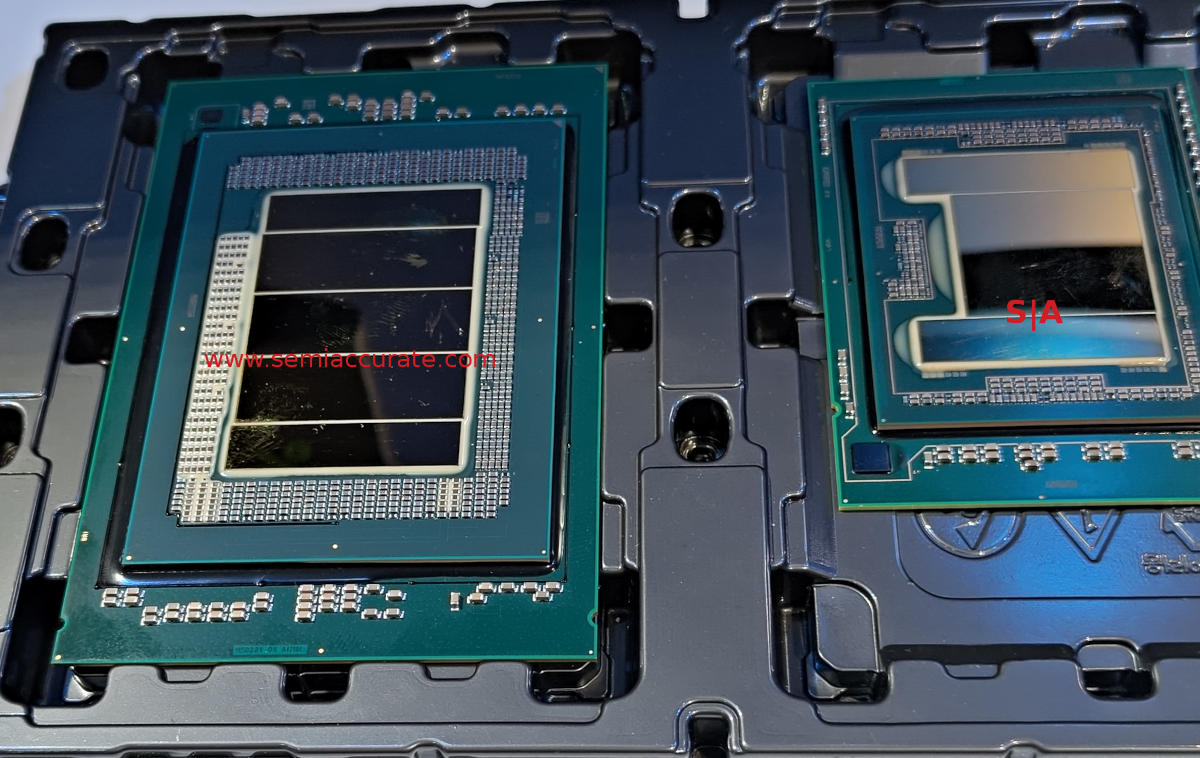
When we first saw Clearwater last fall in Arizona, we noticed it was sitting on a small PCB which was sitting on a larger PCB. Around the silicon/chiplets there was a light colored underfill with a darker one between the two PCBs. It seemed like an overly complex choice that added cost but the answer we got turned out to be anything but.
Two PCBs for one CPU
To the surprise of no one, you need a very high quality substrate to mount multiple high end chiplets, even with EMIB bridges. Clearwater Forest is also a very big CPU with a lot of power and data pins running at high speeds so it needs a very big PCB to fit in a very big socket. A PCB that will do this needs high quality materials and lots of layers, both are industry synonyms for expensive. That little PCB is very high cost little PCB.
The smaller PCB the silicon mounts to doesn’t have sufficient space to put all the pinouts needed for the CPU to socket connection without making the spacing far too narrow to be practical in the underlying socket. The solution? Spread out the pins. How? With another PCB obviously, which also allows you to add more passive components too. In short the bottom PCB is a glorified breakout box.
This brings us to the question of why do it this way, why not make that top PCB a bit bigger and avoid the multiple additional packaging steps and attendant costs? Remember when we talked about how those high end substrate materials were expensive, and I mean really expensive? It turns out that making a single PCB from those materials in the larger size is significantly more costly than doing things in a two tiered approach. Think shrubbery.
So the long and short of this complex sounding packaging solution for Clearwater Forest is not deeply technical engineering, it is money. Doing one big PCB from expensive materials costs more than two layers, one smaller and expensive, one larger and cheaper. Since it is buried under a metal heat spreader, chances are no one would ever notice, but if they do, there is an easy explanation.S|A
Charlie Demerjian
Latest posts by Charlie Demerjian (see all)
- Intel Cuts HDR OLED Panel Power with SmartHDR - Apr 2, 2026
- ASBOtech Makes A Real-World Useful Smart Ring - Apr 1, 2026
- Why Does Clearwater Forest Have Two PCBs? - Apr 1, 2026
- Intel Celebrates vPro 20th Anniversary With New Hardware And Software - Mar 25, 2026
- Anritsu Has The Nicest Testers At MWC - Mar 16, 2026