![]() Japanese memory manufacturer Elpida Memory, Inc. (TYO: 6665) has just started sampling some very advanced memory modules.
Japanese memory manufacturer Elpida Memory, Inc. (TYO: 6665) has just started sampling some very advanced memory modules.
These modules use TSV – short for Through Silicon Via – to stack individual chips on top of each other thereby reducing the footprint required for the module.
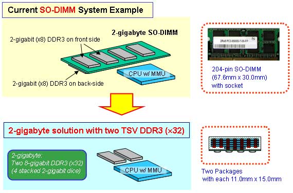
Traditional modules are manufactured using the well known SO-DIMM layout from notebooks, but in many cases manufacturers of consumer electronics would prefer to solder the memory module directly onto the motherboard.
As can be seen on the illustration provided by Elpida, the new memory modules have a capacity of 1GB and 2 of these can replace a single SO–DIMM of 2GB.
TSV is a technology where you have conductive copper channels vertically through the entire chip. When you stack multiple chips on top of each other, these channels will make contact with each other allowing current to flow from chip to chip.
This technology can be contrasted to the traditional method of using wires along the edge of the chip. TSV reduces footprint to a minimum, but at the same time requires very precise manufacturing.S|A
Full press release can be found here.
Mads Ølholm
Latest posts by Mads Ølholm (see all)
- Samsung shows off 20nm PRAM - Feb 28, 2012
- DDR4 shows up in the wild - Feb 28, 2012
- SanDisk develops the world’s smallest 128Gb flash chip - Feb 22, 2012
- Aussies create single atom transistor with precise control - Feb 21, 2012
- Chinese 16 core CPU uses message passing - Feb 21, 2012
