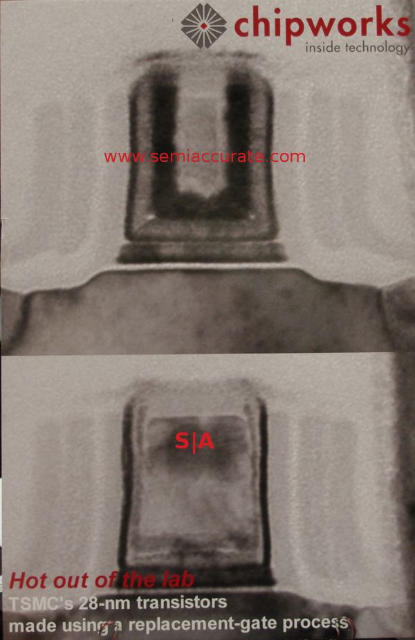
![]() The final piece of the TSMC 28nm HKMG process puzzle was put in place at SemiCon last week, it now makes sense. Chipworks got ahold of a Xilinx Kintex-7 FPGA, and it revealed a few secrets on the operating table.
The final piece of the TSMC 28nm HKMG process puzzle was put in place at SemiCon last week, it now makes sense. Chipworks got ahold of a Xilinx Kintex-7 FPGA, and it revealed a few secrets on the operating table.
If you recall, AMD is on track to put out Southern Islands chips much earlier than most people, SemiAccurate included, expected, possibly even this quarter. The real question is what process they are going to make it on, the TSMC 40nm SiON or 28nm HKMG? 40nm would be big, hot, and limited, think volcanic island more than Southern, while the 28nm SHP HKMG process wasn’t supposed to be ready until late Q1, best case. The short story is that Southern Islands is very likely not on either one.
That leaves the 28nm SiON aka 28nm LP, something that may be viable for a low power ARM SoC, but not a high power GPU. SiON at these geometries is far too leaky. Enter the good folk at Chipworks, and the poster they had at their SemiCon booth. They had just finished taking apart an FPGA based on a 28nm TSMC process, and guess what they found? HKMG. Sort of.
Cluetrain hits at Semicon
The short story is that there is another process, and one that is not talked about much, 28nm HPL, or 28nm low power with HKMG. That is what Xilinx uses, that is what is likely in Apple’s chips, and that is what AMD will almost assuredly use too. If you want all the details, the Chipworks blog post on it is here, and you can buy the report here. Low power does not necessarily mean what most people think it does, just that the process is tuned for different sweet spots than the high performance process.
Our sources have been saying that the TSMC 28 HP process is not doing well for a while, and checks before Semicon confirmed their stance. Given the large difference between the two processes, SiGe being the likely one, it looks like HP is still somewhat problematic.
What this means for the GPU set is pretty simple, it is better than the 40nm SiON process, but not as well suited for the segment as the 28nm HP process would be. If you can use it for your chip, and AMD looks like they can, then you are not going to wait for the HP process to come out some six months later.
Given the late Q1, maybe, time frame for Kepler, it looks like that part will be on 28 HP. One related point, low power tends to mean lower clocks, and Nvidia runs their shaders at 2x the base clock, in the neighborhood of 2x what AMD runs theirs at. This may be the key differentiator that enables AMD to use 28 HPL while Nvidia’s architecture may be unsuitable.
Short story, AMD is coming out with Southern Islands soon, Nvidia and some lower end SI parts are probably gated by TSMC’s 28 HP process. We know why Q3 is going to be an exercise in pain for Nvidia, and if the information above pans out, Q4 is shaping up for a repeat. Thanks to Chipworks, we now know how the pieces are lined up.S|A
Charlie Demerjian
Latest posts by Charlie Demerjian (see all)
- Nuvia Founders Have A New Startup, Nuvacore - Apr 16, 2026
- Nvidia Is Negotiating To Buy A Large PC Oriented Company - Apr 13, 2026
- Dell Does Modular Laptop Boards Right - Apr 7, 2026
- Qualcomm Snapdragon X2 Review Embargo Lifts Tomorrow Morning - Apr 6, 2026
- Intel Cuts HDR OLED Panel Power with SmartHDR - Apr 2, 2026
