 AMD just let out some of their MI300 plans albeit in a rather backhanded way. Followers of SemiAccurate will not be surprised by this disclosure though.
In a recent video called Advanced Insights Ep. 2: Sam Naffziger on Modular Design, Sam Naffziger, err, talks about Modular Design. With Mark Papermaster, no technical slouch himself. In short there is a 25 minute conversation between two people who get the tech and don’t dumb it down too much. It is well worth the watch. The interesting bits aren’t explicit however, you have to have a good understanding of what is happening on the ground before these added tidbits click in to place.
There is a lot of talk about AMD’s historic use of chiplets and modularization, things which in some ways can trace their lineage back to Llano and the first few APUs named after streets in Austin, TX. That bit of history isn’t in the video but we will forgive them for this glaring oversight even if the Austin Bureau of Tourism and Wanton Firearms Discharging won’t. Long story there that we don’t feel like making up at the moment so on with the show.
If you look back to AMD’s modern history with chiplets, the first Naples Epyc CPU was a bit crude by modern standards but it worked really well. Design a chip that would operate on it’s own as a consumer part but could be placed on a PCB 1, 2, or 4 times to make a coherent whole. You get a single small device that is much easier to validate, has much higher yields due to size, but gives up a bit in terms of areal efficiency. Basically all those PHYs and logic needed to glue the chips together take up area that wouldn’t be needed if the device was a monolithic design. And they eat power too, whether needed or not.
So you give up area and power for every device but you only have to make one device, not four, to satisfy the entire market. AMD put out an ISSCC paper in 2021 that claimed an ~10% net die area increase over a monolithic design offset by a net 59% cost versus monolithic. While power goes up too, there are ways to minimize that, and, well, chiplets are a clean kill. At this point the ‘old ways’ were dead for many markets.
The follow on device, Rome, took things much farther with the functionality split into different chiplets. You could make a solid argument that the chiplet era began with Rome, it used heterogeneous chiplets, chiplets on differing processes, had multiple configurations of chiplets, and was reusable for consumer devices with little more than a chop of one chiplet. Oh yeah, those consumer CPUs were modular too with 1 or 2 CCD options as well. Instead of making a monolithic die at reticle limits with yields that necessitated a lot of less than fully configured devices, AMD made an 80-something mm^2 chiplet on a current process and a larger one on an older process.
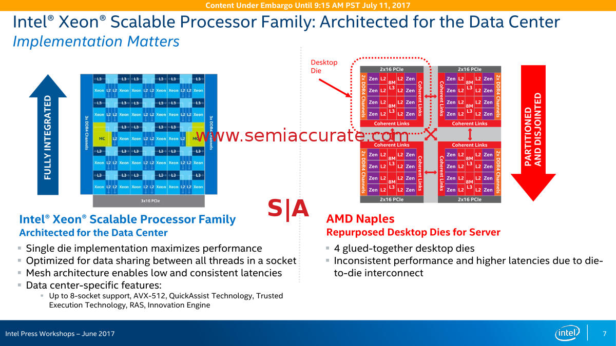
Playing Lego with the components meant dozens of CPUs across all markets with three, 2.x really, designs. And they kicked Intel to the curb with the result. Well to be fair Intel helped out quite a bit by falling on their face with process ‘whoopsies’, but AMD would have done pretty well without this generous assist. Performance up, costs down, use of scarce wafers on high demand nodes down, and flexibility of SKUs at a previously unbelievable level. Downsides? The aforementioned die size increase and added power which was significantly reduced this generation. As a bonus, we got to pull this slide out again and ask questions like, “who won again”, and, “This is why we told you not to use it”. Yeah it was cathartic.
I think they meant Sapphire Rapids, not Naples
With each new generation there were advances, the 3D stacked cache on Milan and Genoa, not to mention the consumer versions, were a much bigger step than most people realized. With a minor change to the top metal layer, AMD got 3x the L3 cache and blunted Intel’s HBM CPUs in the market for a fraction of the cost. Bonus: Gamers got a chip that, well, wasn’t very good but some believed it was. We will reiterate, if you are going to make and enthusiast/gamer part, don’t nuke overclocking, learn from Intel’s mistakes.
So in the end, AMD took a monolithic design and made it cheaper, faster, more capable, flexible, and turned the initial weak points into rounding errors. But that was just the beginning. If you recall this article is purportedly about MI300, right? What does that have to do with anything? Well MI300 is both the pinnacle of AMD advanced packaging and the beginning of a new era. The key to it was the planning that went into the device long before any silicon was designed. This is touched on in the video but the real depths of the planning haven’t been outed publicly as far as SemiAccurate is aware.
MI300 is not really a device, it is a flexible architecture. If you want to pin the name to any single chip, the base IOD is the heart of the line. Those dies are essentially I/O, HBM memory controllers, and pins out of the top. Those pins can have anything 3D stacked on them, they are not directly tied to a partner chiplet design. Actually they aren’t tied to a single partner chiplet either, there are two or three per IOD in the current MI300s.
The original MI300 had three IODs topped with GPUs and one with CPUs, the pleural is because there are actually two GPU chiplets per IOD or three CPU chiplets. The or is important because if you recall, both Intel and AMD had hybrid CPU/GPU devices coming out about the same time. Intel had Falcon Shores, AMD MI300 with a suffix. Intel very quickly reversed course and Falcon Shores became GPU only much to the scathing commentary of the couch borne commenterati. AMD followed suit quickly with a 4x GPU bearing IOD version of MI300, different suffix, with far less commentary from the mumbling masses.
What was clear was that this wasn’t a screw up from either side, it was a glimmer of recognition among the customer base. The important bit is that both Intel and AMD could pivot their architectures very quickly and ended up with a full GPU version of their offerings with almost no silicon redesigns. Prior to chiplets, this would not have been possible in the time frames needed, period.
So AMD went from a 3:1 GPU:CPU device to a 4:0 with literally no silicon changes and did so in months. There are rumored versions with 0:4 too, basically an HBM version of Genoa. There are also versions strongly rumored to carry Xilinx FPGAs as well, something that some pundits scoff at. If you can make an FPGA chiplet with the correct pinouts, what is the problem again? GPUs are probably the worst case for thermals and power so just about anything else will probably work. The protocols for the IOD to CCD/GCD(?) are well documented (GMIx) so the problem once again is…?
Anyway back to the story, what future plans did AMD reveal in the video? Hold on to your hats, this one is big now that you get the back story.
Note: The following is for professional and student level subscribers.
Disclosures: Charlie Demerjian and Stone Arch Networking Services, Inc. have no consulting relationships, investment relationships, or hold any investment positions with any of the companies mentioned in this report.
Charlie Demerjian
Latest posts by Charlie Demerjian (see all)
- Intel Bumps Xeon Memory Speeds - Jul 20, 2026
- Qualcomm’s 2026 Investor Day Has Hidden Goodies - Jul 15, 2026
- Phison Phudges The Numbers… In A Good Way - Jun 24, 2026
- Who Are The Qualcomm Enterprise Customers? - Jun 23, 2026
- Innodisk Adds 10GbE To Useless M.2 Slots - Jun 19, 2026