![]() Intel is finally taking the wraps off of Knights Corner, the product now known as Xeon Phi. Today the cards go on sale to the general public, and some but not nearly all of the specs have been released.
Intel is finally taking the wraps off of Knights Corner, the product now known as Xeon Phi. Today the cards go on sale to the general public, and some but not nearly all of the specs have been released.
Last August at Hot Chips 24, Intel talked quite a bit about the microarchitecture of Knights Corner, a bit about coding for it, and gave a vauge outline of the uncore, but the product itself was kept under tight wraps. Luckily, SemiAccurate got a good chunk of the specs at IDF, but not nearly all. With today’s disclosure, the product specs are outed, a lot more on the software/coding front comes out, but sadly, Intel did not respond to questions about the die size or any deatials on the arrangement of the chip. The most detailed data we got from Intel in this regard is a transistor count of about 5 billion.
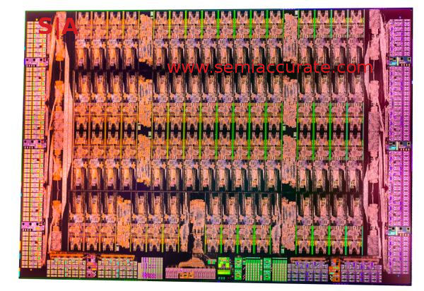
The die in all it’s glory
Knights Corner (KC) has a most unusual core count, 62, and the reason behind that binary unfriendly number is decidedly non-technical. Why 62 cores instead of 64? That’s what fit on the die. No, we are not joking, if you look at the die shot above, most of the repeated units all have eight cores around a central unit. Seven of these blocks have four cores on each side, two sets per horizontal row. The lowest row has an unidentified unit in the middle that takes up enough room to crowd out a couple of cores.
Our guess, and Intel would not go into any detail here, is that the eight cores surround a memory controller. Intel has previously stated that cores have a physical affinity to a memory controller, so this, a ring stop, and eight cores make a nice logical and repeatable unit. The odd blob in the middle is quite likely to be a ring stop and associated logic for the I/O and PCIe controller. Around the edges we have the physical interfaces to memory and PCIe. For the curious, the graphics portions of the chip are still physically present, but have been hard fused off and power gated so you can never access them.
Some of the specs, not nearly all though
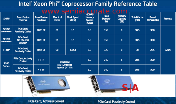
That brings us to the card itself, or in this case cards. As with most modern chips, KC has been turned in to a bevy of different products, in this case five. If you discount different cooling mechanisms, there are only three real variants, the 3100 series, the 5110P, and the SE10 ‘special edition’ cards. These last two are essentially purpose built parts made for the TACC Stampede supercomputer and related projects. You won’t be seeing them for sale in the wild, but they are likely very close to what we showed you at IDF.
Next on the list is the card being officially released and sold today, the 5110P. This one cedes one core, 47MHz, 500MHz memory clock, and 75W TDP to the SE10 line, but that only about 6% in total. This card is aimed at the compute server market, so it is passively cooled, but still delivers a hair over 1TF DP FP from 60 cores. Memory is 8GB of 5GHz GDDR5, dropping to a claimed 7.75GB usable with ECC enabled. For the low low price of $2649, you get all this in a pretty blue metal shroud.
One step sideways from there is the 3100 line, and these are aimed at workstations rather than compute servers so it has both active and passive cooling solutions. This line loses two memory channels and the 2GB of GDDR5 that is associated with them, but the GDDR5 speed remains the same. Core clock and core count is not specified, and neither is performance but you can assume it will be set to beat the competition when it goes on sale. Since TDP goes through the roof to 300W even with the decreased memory, you would be pretty safe in assuming the clocks go up substantially.
Luckily for us, the censors at Intel are not math enabled, if they were, they would probably realize that each core has an associated L2 cache. The 5110P has 30MB for 60 cores, the SE10s have 30.5MB for 61 cores, and the 3100 line has 28.5MB of cache. A bit of math puts the core count at a nice even 57, with “nice even” being defined as “not prime like 61” in this case. All this, whatever Intel defines “this” as for the 3100 line, can be yours for a mere, “under $2000” some time in the first half of 2013.
All the cards are connected to a rather interesting bus, it uses PCIe2 signaling but runs at 7.1GHz, very close to the 8GHz of PCIe3. Other than that, it is a pretty standard accelerator card for HPC and generic number crunching. It looks like a cluster of x86 servers that are on a TCP/IP network, and takes almost no programming expertise to port to. Optimization is very similar to a standard x86 CPU, and you can use the Intel tools that are very well established in the HPC world. Plug and play is not a misnomer here.
In the end, you have a very powerful card for notably cheaper than any of the competition. More importantly, you can run your code on it with almost now tweaking if it is already thread aware. The learning curve from the hardware and software side is very very low, and that is going to shake up the market. Six years, six months, and two days after this author first wrote about the project, you can finally buy something from the Larrabee project. About time.S|A
Charlie Demerjian
Latest posts by Charlie Demerjian (see all)
- Nuvia Founders Have A New Startup, Nuvacore - Apr 16, 2026
- Nvidia Is Negotiating To Buy A Large PC Oriented Company - Apr 13, 2026
- Dell Does Modular Laptop Boards Right - Apr 7, 2026
- Qualcomm Snapdragon X2 Review Embargo Lifts Tomorrow Morning - Apr 6, 2026
- Intel Cuts HDR OLED Panel Power with SmartHDR - Apr 2, 2026

