Author’s note: This architecture article is incomplete. Due to some quirks in the disclosure of information about Bulldozer, some information was released early, some will come in the future. This article covers only the information released at Hot Chips 23 in August, the rest will have to wait. The holes will be filled in as soon as the embargoes lift, and don’t worry, it annoys us too but out of respect for briefings, NDAs and our fellow journos we will restrict our coverage to public information at this time. Apologies in advance.
 Bulldozer is one of those industry legends, an architecture that has grown far beyond anything the silicon could ever be. Just what the core is technically, and what it is not, is the subject of the following article.
It has been a long time since this author first wrote the name Bulldozer, April 28, 2006 to be exact. (Note: No links due to this, sorry). During those 5+ years, bits and pieces have emerged, projects have been canceled, and changed, but the chip is still not out yet. If rumors are to be believed, it won’t be long now, but sadly, we can’t confirm or deny those officially.
During the always excellent Hot Chips conference this year, AMD’s Sean White gave a talk about the architecture, and only the architecture, of the new CPU. To say it is different is understating things, it is really a bold step into places where few have gone, and no one has tried on a consumer product. The closest thing to AMD’s new Bulldozer architecture out there is Sun’s Niagara, and no one would accuse those designers of following the pack.
What makes Bulldozer so different when the current ‘Stars’ core, and it’s predecessors, is fairly conventional? Instead of using some kind of SMT/threading scheme to increase thread count, AMD did something that most consider ‘thinking outside of the box’. The architects of Bulldozer simply put in two integer (Int) cores, and a single wide floating point (FP) unit is shared between them. Basically it uses two cores for two threads, not one. There is simply no consumer CPU that does anything remotely similar.
Whether the end result is a good thing or bad is going to have to wait for hard numbers, but there is no shortage of ill-informed opinions all over the net. Unfortunately, as we said in the introductory note, we can’t talk about that. Yet. So with that, lets look at the place where the devil resides, the details.
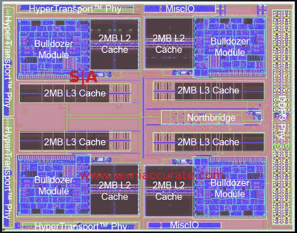
Floor plan of Bulldozer
The floor plan doesn’t really look like it is very odd, it looks like a very conventional 4 core CPU, but there are two interesting bits. The first is the cores are listed as Bulldozer Modules, not cores. That is because of the second interesting part, this is an 8 core device, each of those modules are a pair of cores, not one. They are very tightly bound together, so tightly that there is a fierce debate raging as to what defines a core.
Core is a rather interesting point of contention in the CPU world, and the lines to define it have been blurring with every new architecture released. What used to be a synonym for socket has been so thoroughly abused by laymen, PR people looking for a headline, and just about everyone in between that it is almost meaningless.
That said, for the purposes of this article, we will define a core as an integer pipeline that has it’s own instruction scheduler and can operate in a completely independent fashion from any other ‘core’. If you take the other out, the first core will still be fully functional and not lose any performance.
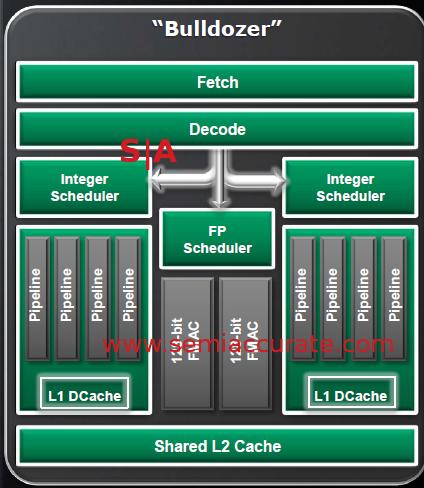
Bulldozer was designed with a philosophy that can be summed up as a mashing together of two cores, some parts are now shared, other still discrete. Parts that could be shared between the cores in a module with little to no loss in performance were, and parts that can’t be shared without a lot of pain are still discrete. The end result is that the integer pipes were kept separate, but the FP unit was shared, as was the front end and the L2 cache. Bulldozer had a long gestation period, more than five years since the author first heard the name, so presumably AMD had the time to do things right here.
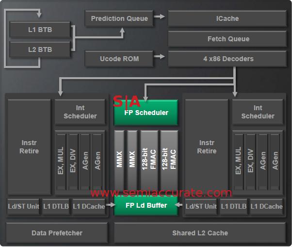
Bulldozer core diagram
From there, functionality of the shared parts was beefed up, allowing those units to service two cores without becoming a bottleneck. If done right, this has a minimal die area cost, far less than duplicating a unit for each core. The front end is a good example of this, both cores share an L2 cache, so why should each ‘core’ have a separate TLB? Bulldozer can be seen as a case of methodically looking at each part of the core, and merging what they could, where they could where is made sense.
One of the dark secrets of a modern CPU core is that in order to keep performance high, there are far more resources on the chip than can actually be used at any given point. If you want high integer performance, you need to have enough Int pipelines to execute all the instructions that the front end can feed in. Same for FP pipelines. If you do make a chip with all those resources, during integer heavy workloads, the FP units are simply idle. During FP workloads, the Int units are idle, so a large portion of the die is basically wasted.
The key to modern CPU design is to balance things as best you can based on expected workloads. It is a big trade-off, a colossal game of move-the-bottleneck played out on CPU simulators and barstools. When you are satisfied that your proposed design will do what you want, you set about making it as efficiently as you can. Years later, when silicon comes out of the fab, hopefully things worked out, and the world hasn’t changed under your feet.
Back to Bulldozer. Optimistically speaking, if the designers did right, each core in a module will have no worse performance than a hypothetical single discrete Bulldozer core, but take up less area than two of those. Best case, each core will have 2x the resources of a single discrete core at no ‘cost’. The FP unit is a good example of this concept, it could really shine under certain workloads.
If those crystal ball gazers didn’t do their work, the worst case is one side bottlenecks the other, stealing resources, thrashing caches, and destroying performance for both cores. Per core performance/mm^2 from a shared architecture could range from amazing to horrid, the end result depends on so many variables that it is almost hard to fathom.
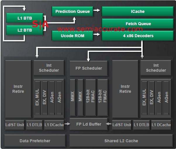
Bulldozer front end
Bulldozer has a shared front end. That means all the data that hits the module comes from one place, and that place is generically known as the front end. The L2 cache, some L1 caches, fetcher, and x86 decoders are common for both cores in a module. Each integer unit has it’s own distinct instruction scheduler, making it a real ‘core’ as we mentioned earlier.
Probably the most interesting thing, other than the shared components, is that AMD decoupled the fetch logic from the prediction logic. Performance of modern CPUs is very dependent on how well it can get instructions and data from memory. Modern CPUs run in the GHz range, memory runs at hundreds of MHz, so the latency when reading from memory can make things very painful. The time between a CPU requesting something from memory and when it arrives can be literally thousands of clock cycles. During that time, a CPU just sits there idle, burning power while doing nothing useful.
L1, L2, and L3 caches are all there to minimize this, a cache miss can be utterly devastating to performance. Out of order execution can hide some of this wait, but nowhere near enough. Almost every modern CPU has some sort of logic to predict what the core will need next, and put it in the lowest level cache possible. If it works perfectly, the CPU should always have what it needs, before it needs it. Prediction and prefetching are probably the two hardest things to do right in a CPU, and even a tenth of a percent gain in efficiency can have a massive effect on overall performance.
Normally, the predictor and fetcher are one unit, it predicts what the CPU will need and then gets it. To eke that last bit of performance out of the CPU, AMD decoupled the two features, the predictor can predict what the CPU needs, and the fetcher can go out and get it, but both can operate independently of each other. With luck, this will greatly increase accuracy, and boost performance, or at least avoid a few more crippling waits for main memory.
AMD wasn’t giving out a lot of information on this predictor, it is seriously in to ‘secret sauce’ territory. A little sleuthing came up with some details, and it looks like Bulldozer has two different and independent methods of predicting the data the fetcher will then get. These methods can be seen as fast and slow, and are likely fired off simultaneously. The fast predictor trades speed for accuracy, a very common architectural trade-off. The slow variant is the opposite, and that explains the names.
If a predictor identifies the correct data, and the fetcher gets the data before the CPU needs it, then everything works out. If the predictor guesses wrong, or the data isn’t pulled in before the CPU needs it, you can have a lot of very bad things happen, the least ugly of which is the CPU just sits there for a few hundred cycles before it can do anything. Penalties for a miss range from bad to horrific in terms of performance loss, there is a reason that modern caches are so big.
The results of the predictions are placed in a queue, and those are then pulled from main memory whenever the fetcher has the time to act on them. This means the fast predictor will put an answer in the queue in short order, and the fetcher should always have something to go out and get. Once the result of the fast predictor is fetched, that is the end of things, it likely signals the slow unit to abandon work on the same instruction.
Hopefully the fast logic got the answer right, but predictions aren’t always accurate. Magic starts to happen when the fetch queue starts to build up, giving the slow unit time to complete a more accurate prediction. If the fast result is still in the queue when the slow unit gets done, it replaces the result with a hopefully more accurate one.
In theory, this scheme of Glewing two or more units together gives you the best of both worlds, speed and accuracy, and has no downside. More importantly, the decoupling means you can implement whatever you want for predicting, if you want to run many more algorithms, that is your choice, just think through the trade-offs. The take home message is that the scheme is expandable.
For sheer numbers, the ICache (Instruction Cache) is a 2-way 64K design, and it is filled by 32 byte fetches. Each core/thread has it’s own prediction queue, quite a necessary and obvious duplication. The instruction ITLB (InstructionTranslation Lookaside Buffer) is 72 entries for the L1 cache, 512 entries for the L2. L1 BTB (Branch Target Buffer) is 512 instructions long while the L2 BTB holds about 5K instructions. In addition, Bulldozer’s front end can fuse branch instructions to save space and increase performance.
The last step is the x86 decoder, and there are four in Bulldozer. That means that instructions are issued to the ‘cores’ in an interleaved fashion four at a time. Worst case, a core effectively is able to get 2 ops/cycle, but if the other core is idle or waiting on memory, the other could theoretically get more than the minimum number.
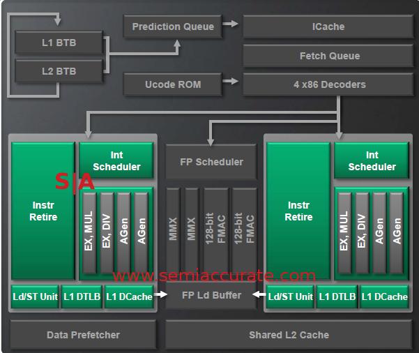
Bulldozer Integer units
That brings us to the heart of the core, the integer units. This is the one part that is not duplicated, each is considered by AMD to be a core. Each core has it’s own instruction scheduler, so it works completely independently of it’s twin on the other side of the module. Nothing is shared here, a core is a core, but they still only come in pairs.
In case you didn’t notice, the front end doesn’t have an L1 DCache (Data Cache), each core has it’s own 16K DCache. To back this up, each core has a DTLB (Data TLB), it has 32 entries and is fully associative. This is the long way of saying instructions are fetched, decoded and fed to the cores from a shared asset, but each core keeps it’s own data, and keeps it close. This is an obvious thing to do to keep from long waits for critical data, there probably isn’t a sane way to share these caches and keep tolerable performance.
Each core also has it’s own load/store logic too. This unit is fully out of order with a 40 entry load and a 24 entry store queue. It can issue two 128-bit loads or one 128-bit store per clock, but no word on how the controllers upstream determine what to act on.
Both integer cores share a write through L2 cache, described by AMDers as ‘mostly exclusive’. The L3 is exclusive and shared among modules, but that is attached to the north bridge, not in the modules themselves. There is 2MB of unified L2 per module, 8MB total across first 8 core chip, and it is 16-way associative. TLBs for the L2 are 8 way, 1024 entry units, and it has two page table walkers for obvious reasons. All of this is serviced by multiple prefetchers, but there is no word on what schemes they use to do their job, but the prefetches can be non-sequential.
All in all, the L2 can keep track of 23 cache misses at once, probably enough to handle most tasks. Interestingly, the requests for information that miss from the L1 are simultaneously fired off to the L2 and main memory to hide latency. This reduces potential latency, but costs a lot of bandwidth. If it helps the prefetchers keep the caches full, it is well worth the trade-off, most improvements here are.
Bulldozer FP unit
That brings us to the oddest part of the architecture, the FP unit. It is shared between the two Int units, and is seen as a coprocessor, not an integrated pipeline like almost every other modern CPU. This means that any FP instruction will be fired off to the shared FP scheduler, there is only one, and when the instruction is completed, the FP unit signals the ‘core’ that it is done.
Remember those added resources that were mentioned earlier? Currently, the ‘Stars’ cores have a 128-bit FP unit. With Bulldozer, there is one FP unit that can crunch two 128-bit numbers per clock. The shared scheduler means there is a single central arbiter that can make sure things are ‘fair’ to both cores, but if one core doesn’t use an FP instruction that clock, the other core can use twice the resources it is usually allowed to.
What this means is that the FP unit should be more than capable of reaching the ‘best case’ scenario for the shared resources as long as the other core isn’t doing any FP work. For non-HPC work, this is very likely to happen, and better yet, if you purposely idle one core per module, you end up with an FP monster with lots of bandwidth to feed that unit with.
AMD considers this to be a killer feature of Bulldozer, and for many HPC workloads, the chip should fly. Consumers probably won’t notice this as they don’t tend to have optimized and sustained FP workloads. That said, it will be interesting to play around with benchmarks here once the tools come out that allow users to hand tune the cores and exploit this potential feature.
Bulldozer supports AESNI, AVX, and a few unique features called XOP and FMA4. If you recall, AMD announced an instruction set they called SSE5 preemptively. Intel didn’t like this much, so their post SSE4 instructions became SSE4.1, SSE4.2, and then AVX. SSE5 was AVX plus XOP and FMA4, so Bulldozer is a superset of what Intel’s Sandy Bridge CPU supports with one exception.
That exception is FMA4, Intel has a variant called FMA3 in Haswell. FMA or Fused Multiply-Add is just what it sounds like, a multiply and an add in one instruction. The difference between FMA3 and FMA4 is the number of registers it uses, in this case, three or four. If you are doing a multiply and an add, you have to use three numbers, (A * B) + C, each stored in a register. FMA 3 puts the result in one of the data registers, usually C, and FMA4 puts it in a different register, lets call it D. FMA 3 overwrites one register, FMA4 doesn’t.
Update: Intel won’t have FMA3 until Haswell, not Sandy Bridge as indicated earlier.
FMA operations tend to be done in large quantities, and FMA4 allows you to save one load per operation because it doesn’t overwrite anything. This can be a massive time saver, and everyone SemiAccurate talked to said that FMA4 is a clean kill over FMA3 for HPC applications. Piledriver or ‘Enhanced Bulldozer’ also supports FMA3 as one of the enhancements. Look for that core to debut in Trinity next year.
That about wraps up the architecture of the Bulldozer module itself. The module is by no means the complete CPU, there are currently four modules on each die, along with an integrated north bridge, L3 cache, memory controller among, and much more. What are they? How does it all perform in the real world? Was it worth the wait? When will it be launched? Those are all good questions, but ones we can’t answer yet. Luckily, there is an indeterminate, but not terribly long, time to wait until we can. Soon.S|A
Charlie Demerjian
Latest posts by Charlie Demerjian (see all)
- Qualcomm Is Cheating On Their Snapdragon X Elite/Pro Benchmarks - Apr 24, 2024
- What is Qualcomm’s Purwa/X Pro SoC? - Apr 19, 2024
- Intel Announces their NXE: 5000 High NA EUV Tool - Apr 18, 2024
- AMD outs MI300 plans… sort of - Apr 11, 2024
- Qualcomm is planning a lot of Nuvia/X-Elite announcements - Mar 25, 2024
