 The question of what would happen if you built a Pentium on a modern process was answered during IDF 2011. Unfortunately it wasn’t actually explained until Hot Chips this year, the initial demo was a PR exercise in distraction.
You might recall the “solar powered CPU” nonsense that Intel put on at that time, it was an masterclass in headline grabbing while belittling your own accomplishments. Intel got lots of headlines, and they were almost all wrong. To the best of SemiAccurate’s digging, the number of stories that explained what was going on was one. Even with that, the name Claremont was never mentioned, nor were any real details.
Since that changed at Hot Chips, we figured it was time to fill you in on what was missing at IDF, or at least some of it. We will leave out a lot of the EE and design methodologies, that is something we don’t cover, and stick to the chip itself. The goals, results, and how far the team who made Claremont came is still quite a story.
You might recall that the original P54C that debuted in 1994 was the .6μm BiCMOS successor to 1993s .8μm P5, the original Pentium. It initially ran at 90MHz on a 60MHz bus, and pulled a whopping 9W at 3.3v. From here, the numbers get a little sketchy, but it used about 3.3 million transistors and took roughly 147mm^2 of die space. It was Intel’s first superscalar CPU, and brought other bleeding edge technologies down to the consumer level as well. This was hot stuff two decades ago, and its design is the starting point for Claremont.
The designers of course had an agenda, but it wasn’t hidden, it is actually slide two of the Hot Chips presentation they gave. Bad puns aside, the goals were to make a near threshold voltage IA CPU, and extend the dynamic range of operation from there to Vmax. They wanted to do this while pushing low voltage, variation aware, multi-corner design methodologies too, and that is the part we will mostly gloss over. The first two are more than interesting enough.
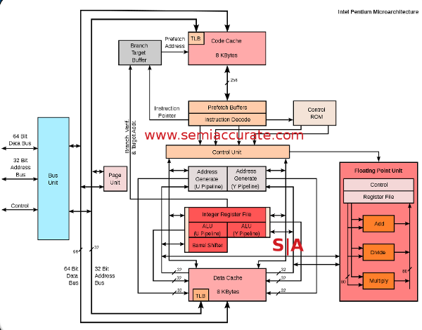
Pentium P54C core diagram
As you might recall, the P54C eventually clocked between 75 and 120MHz, bus speeds were either 50, 60, or 66MHz, and the core ran at either 1.5x or 2x that speed. Memory ran at half the bus speed on a 64-bit wide bus, another first for Intel. All of these clocks were fixed, and could not be dynamically modified, so no sleep states, and no turbo, just the set clock rate that spanned a mere 45MHz range top to bottom. All those power management, clock gating, voltage domains, and other nice features we now take for granted simply were not there in P54C, it is what it appeared to be.
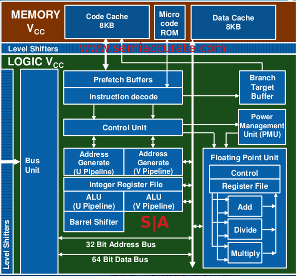
Claremont core diagram
Step forward to Claremont, a slightly more modern interpretation of the P54C core done in 32nm CMOS, not BiCMOS. It has a design target voltage of .5V for the core logic, more obviously for the I/Os that need to interface with the older mobos, and an aimed for <20mW total core power draw at that level. There were now three optimization points, not one, .5V@66MHz, .75V@333MHz, and 1.05V@525MHz, and the cores had to be clock variation aware. As you can see, this is not a simple re-layout, it is a comprehensive redesign of the old logic to push the boundaries of modern circuit design tools and technology.
To start out with, what did they do? First they added power management, different voltage planes for I/O, instruction driven power gating, turned off the FPU totally when not in use, and did all of this with a one cycle wake up period. The sleep thresholds are fully programmable, application aware, and variable based on operating points of the chip. If you think about the changes needed to go from no power management to instruction driven power gating, it is more than a slight difference, closer to a completely new chip.
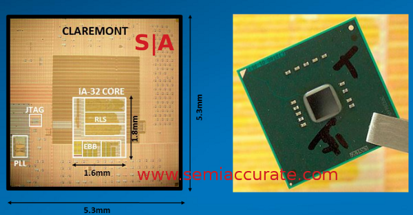
Note the tweezers on the right
So, glossing over what the engineers needed to do to make the above happen, how did the results turn out? It works pretty well, if you recall that ‘solar powered CPU’ demo, you might have seen it running yourself. Claremont on 32nm has 9 metal layers, 6 million transistors, and the core consumes a massive 1.96mm^2 as part of a larger package. That is likely for compatibility with existing Pentium motherboards, and it uses a custom interposer to go from its native 951 pin FCBGA11 package to a standard Socket 7 pinout, and because it would be totally pad bound at that size.
Power and speed curves
So far so good, but how well does it work? A little better than expected, clocks start at 10MHz and go to 741MHz, an almost 750x range, voltages run from 380mV to 1.1V, and the consumes between 1.5mW and 445mW. That is about 20x less than the original did while running at 10x the clock speeds, so better than a 100x improvement in performance per Watt. Not a bad start, and the team beat their stated performance goals handily. As an aside, at 1.1V, leakage is around 3% of the power used, that jumps to around 50% at .380mV.
In the end, the transistor count just about doubled, the area went down by around 75x, and power shrank by about 100x at 90MHz operation. More importantly, Intel was able to run the device at near threshold voltages, and did so reliably. The design methodologies to do this are probably the hardest part of the project, and while the job isn’t finished, Intel now knows how to make a CPU run at the better part of 1GHz, then drop down to nearly zero running at near threshold voltage. I guess you could call this project a success.S|A
Charlie Demerjian
Latest posts by Charlie Demerjian (see all)
- Nuvia Founders Have A New Startup, Nuvacore - Apr 16, 2026
- Nvidia Is Negotiating To Buy A Large PC Oriented Company - Apr 13, 2026
- Dell Does Modular Laptop Boards Right - Apr 7, 2026
- Qualcomm Snapdragon X2 Review Embargo Lifts Tomorrow Morning - Apr 6, 2026
- Intel Cuts HDR OLED Panel Power with SmartHDR - Apr 2, 2026


