 Today Intel is finally launching the dual Haswell server platform called Grantley, all hail the new leader. If you were expecting a simple HT link a second Haswell-E, you are in for a big surprise, these three dies are very different.
Haswell-EP as Grantley is technically called now has a marketing name which rolls off the tongue like a song, Intel Xeon Processor E5-2600 v3. OK, marketing aside Haswell-EP is a damn good platform which really has no competition on the market, it is better than it’s Ivy-EP predecessor in every way. Other than DDR4 and core counts, most of these changes are fairly subtle and why they bring performance to the table may not be immediately obvious. Lets dive in to the details.
The Haswell core has been with us for a very long time, between 12-18 months depending on which launch you count from. We have beaten it’s successor’s trials and travails to death so we won’t go over that, but lets just say the desktop variants are a full generation ahead. That isn’t to say Haswell-EP doesn’t pack surprises, it does, but DDR4 support isn’t one of them even if the name socket R3 is. As with Romley there are four memory channels that are now each capable of up to DDR4/2133 with one DIMM per channel or up to three officially with slower memory. Expect OEMs to push this to four in very short order, the limit of three is mainly official conservatism, a good thing in the server world.
Each socket can support up to 40 PCIe3 lanes or 80 per 2S system. Related to this, QPI is now bumped up to v1.1 which supports 9.6GT/s. This raises an interesting possibility, since QPI is effectively PCIe3 with proprietary overlays, will all the lanes on the 9.6GT/s SKUs clock to 9.6 instead of the 8.0 in the PCIe3 spec? We didn’t have time to test it but winter is coming….
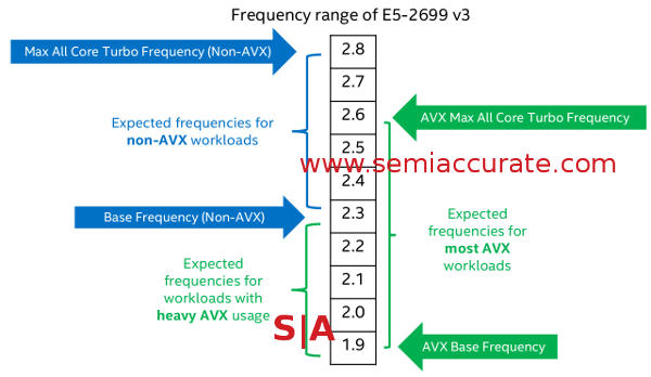
Turbo is also improved both under the hood and in an interesting change, now also affected by the instruction stream the CPU runs. The new mode is called AVX turbo mode and when a Haswell-EP detects an AVX instruction, it goes into AVX turbo mode which drops both base and top turbo clocks by about 3-400MHz for most SKUs. Yes this mode is slower than normal modes of operations, and slows down the entire CPU, not just one core, something which does not happen in consumer Haswell variants.
Here is an average example of AVX Turbo
Most people immediately come to the conclusion that this is a bad idea although some we mentioned it too were far less polite. Luckily for Intel, this initial impression is dead wrong, AVX Turbo mode is a good thing, or at least a better thing than living without it even with those lower clocks. Why? Because Haswell moves from AVX to AVX2 and goes from 8 to 16 DP FLOPS per clock, that would be 128b to 256b wide in human speak.
Since AVX2 Haswell doubles the work done per clock and pays the price by losing ~3-400MHz from a 2-3GHz or so range of parts. 20% for 200% isn’t a bad trade in my book even if some people whine about the minor loss. If you don’t use AVX, you don’t have any slowdown so it is entirely avoidable with a compiler switch. If there are no AVX instructions sent to the CPU for 1ms, the normal clocks take back over too. Why does this happen? Power draw, the more parallel you go, the more work you can do, and the more power it takes. See nearly any GPU made in the last five or so years for more on this topic, they have some pretty creative solutions to the problem too.
I would guess that normal consumer Haswell’s lack this ‘feature’ because the workloads they run are radically different from HPC type workloads that can run heavy AVX code non-stop for days. Consumer parts also have very different power optimization strategies that make a lot of difference to how the chip as a whole pulls in electrons, the AVX problem can be managed differently from that angle too. Consumers are unlikely to scream about clock jitter, HPC and supercomputing users aren’t so tolerant for the most part.
On the power management side there are some pretty large differences between consumer and server Haswells too. The big one is Per Core P-States (PCPS), any core can run at any clock and voltage independently. Consumer Haswell’s didn’t do this, and Broadwell doesn’t do this any more.
Much of this is down to the integrated voltage regulators in Haswell, something earlier Intel CPUs lacked. With no need for an external VR and attendant passives, pins, and all that, you can do much more granular voltage and frequency management. You can also do it faster which brings serious gains in efficiency from sleep modes and other state changes. This is a minor bullet point feature but it does have massive effects on power use and some latencies. It can also drop board complexity, area needed to support a CPU, and therefore cost, but that is pretty minor compared to the cost of the CPUs.
This allows another feature that Intel calls EET or Energy Efficient Turbo and it is a bit of a head scratcher at first. EET monitors core stall behavior and throughput, basically whether or not the CPU is doing actual work or waiting on something external. If the core is mostly waiting on something like memory but has thermal and power headroom, older cores would simply jack up the frequency. Cores then waited on memory at much higher clock rates and this wastes power for no real gain. EET can detect this and stop clocks going up if there is headroom but nothing is to be gained by using it, a very smart way to save energy. Turbo states can also be hard limited to lower variability for sensitive applications like HPC, as we mentioned earlier, some really don’t like jitter.
Another nice feature is that for the first time the uncore on Haswell-EPs can scale voltage and clocks too. Before you say that Sandy-EP could do that too, it could but only in lockstep with the cores. This was because the rings didn’t like being on different clocks from the cores, something that you can probably figure out the causes for on your own. In Haswell the uncore can scale independently of the cores and other way around. Since this feature actually works, SemiAccurate feels that the Haswell-EP validation team deserves a big raise if their therapists ever deem them fit to rejoin society after that task.
In short the uncore now has a turbo mode that is independent of the cores. If the CPU needs more bandwidth or other uncore functions, those clocks can be raised too. Similarly cores can jack up frequencies without pulling the rest of the die up, or if it is the right thing to do, they can all go together when they go.
All this obviously saves power, a theme you will see often on this new CPU. For the record, uncore in this case is defined as the ring and last level cache (LLC) but not the PCIe or memory controllers. More on them later though.
The three Haswell-EP dies, HCC< MCC, and LCC
There are three Haswell-EP dies, LLC, MMC, and HCC aka baby bear, mama bear, and papa bear as the Intel architects probably don’t call them. As you can see they are called “Chops” because they are chops of the same part as the column ironically called “Columns” indicates. The largest of these has 18-cores, 5.69B transistors, and fits in a mere 662mm^2 die. These are huge chips, no they dwarf even monster GPUs while taking a small percentage of those beast’s net power, no small feat there.
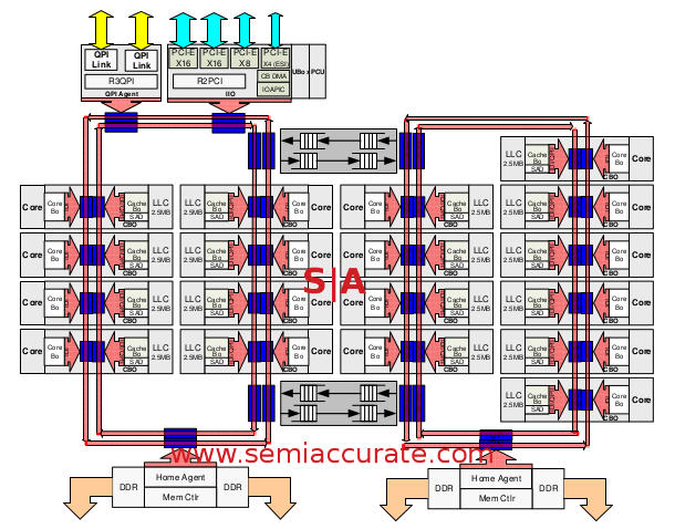
HCC die pictures with four Columns and two Home Agents
As you can see the big die as four columns and is a bit asymmetrical with two rings, two home agents, one set of QPI and PCIe agents, and two rings. You may also have noticed that the ring on the right has 10 cores while the one on the left has 8 cores. Why the asymmetry? In the most technical terms it is because Intel could, there was white space on the HCC die so they added two more cores. That is why you get 18 instead of the nice and expected 16 cores, but the architects were adult enough to not append a, “Nya-nya” to the explanation even if the assembled press couldn’t meet that standard a few times. By assembled press I do basically mean me but there could have been others that I didn’t hear.
You may also notice that there are two buffered switches that act like transparent bridges between the the rings, they do what you would expect and pass data both ways. Since cache data is spread across slices evenly by hashing the address and saving it to the appropriate slice rather than the physically local slice, this happens a lot.
You might expect these switches to add a lot of latency but they really don’t, Intel claims it takes about 4 clocks to cross the buffer and moving the same distance with simple wires would take about four clocks. The buffer is not a simple FIFO though, each does have several virtual and physical channels and each of those acts as a FIFO. This allows Haswell-EP to do a sort of on-chip QoS to prioritize some types of traffic over others, something that comes into play later.
If you take the second ring and chop off the column with six cores, then cap the ring there, you get the mama… err… MMC die. This one has 10-12 cores but is otherwise the same as the HCC die. Please note that this and the LLC are not simple fusings, they are separate dies. The LLC is quite different because it loses everything to the right of the switches including the second home agent, you know that little bit with two of the DDR controllers. Fear not, all of Haswell-EP’s DDR4 controllers can actually support four channels each with little to any loss of performance. Given the core counts though, even a fairly sizable loss would still mean a better bandwidth per core ratio for the LLC in most cases.S|A
Charlie Demerjian
Latest posts by Charlie Demerjian (see all)
- Nuvia Founders Have A New Startup, Nuvacore - Apr 16, 2026
- Nvidia Is Negotiating To Buy A Large PC Oriented Company - Apr 13, 2026
- Dell Does Modular Laptop Boards Right - Apr 7, 2026
- Qualcomm Snapdragon X2 Review Embargo Lifts Tomorrow Morning - Apr 6, 2026
- Intel Cuts HDR OLED Panel Power with SmartHDR - Apr 2, 2026


