![]() Flex Logix, maker of embedded FPGA IP, just announced a new round of funding a few days ago. What does the company do that makes them unique and why is it better than traditional fixed logic?
Flex Logix, maker of embedded FPGA IP, just announced a new round of funding a few days ago. What does the company do that makes them unique and why is it better than traditional fixed logic?
On the funding side, Flex Logix announced they just received $7.4M from Eclipse Ventures, a new investor in the company. Raising new money from new investors is a much trickier thing than getting more money out of existing ones so there is probably something real under the hood. What did Eclipse see that makes Flex Logix interesting to them? We have no idea but the technology the company is producing is interesting to SemiAccurate.
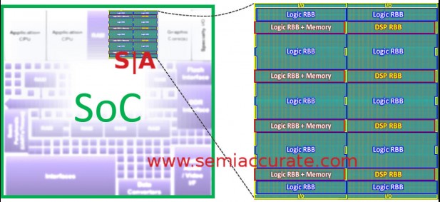
There are two basic products that Flex Logix makes, both under the EFLX banner. The basic part is a FPGA, interconnect, and IO block which is called the EFLX-2.5K when built on TSCM 28HPM. In this guise it takes 1.1mm^2 and give the implementor 2520 LUTs, 5040 flip-flops, 8 clocks, 632 inputs, and 632 outputs. Consider this the basic building block or tile.

Mix and match tiles to your needs
The second variant is called the EFLX DSP core and its main addition is something you have probably guessed by now, a DSP block. For the same area on 28HPM, the DSP drops the LUT count to 1912, flip-flops to 3824, but adds 40 DSP blocks. Each one has a 22-bit pre-adder, 22-bit multiplier, and a 48-bit accumulator but you can chain these reconfigurable blocks to get up to a 43-bit MAC. Much more than that and you probably want to look into more efficient higher level pipelining but for the target markets, 43b MACs should be sufficient.

Memory goes between the tiles
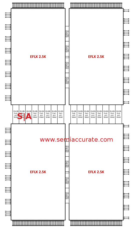
Both of these architectures can be tiled together in up to a 7×7 array if needed. If you want memory, the interconnects between the tiles can have DRAM blocks added to them. An implementor can choose whatever type of memory they are used to dealing with, Flex Logix is memory type agnostic here, it just needs to be TSMC 28HPC compatible. Instead of wiring up the I/Os from one tile to the next directly, the memory is placed between tiles and the I/Os on the periphery of the tile group takes over I/O duties for the entire set.
So why would you want to put a small FPGA into your SoC or embedded controller? It is bigger and less efficient than doing things in dedicated hardware so there has to be a reason. The main reason is quite simply uncertainty and there is a lot more of it then you think. Right behind that comes SKU counts and it’s attendant costs like making masks, it starts to get expensive at 40nm and below 28nm is quite painful. A little more area and expense per chip can end up saving a lot.
To understand what these problems are you have to understand the three main market segments for Flex Logix, networking, wireless/digital front ends, and micro controllers. Each of these has a different reason for using FPGAs in lieu of fixed logic be it uncertainty or costs. While there is some overlap, there is generally a different core reason for each segment.
In the networking side of the market there are two problems, uncertainty of protocols and changing needs. If you are implementing a design for a non-finalized protocol, you have to start your design months or years before the protocol is finalized or wait until it is done to start. Waiting means you are months to years late to the market and someone else is going to free run for months before you are there.
Many specs are written by committee and it is not unusual to find first revisions with portions of ‘hard’ specifications that can be interpreted in multiple ways. Worse yet you could be a small startup that implements things right and the 800 pound gorilla in the market does things wrong and those errors become the defacto standard for the industry. It is enough to make one scream, “IE4”. A little configurable logic in the right places means you can tweak those last-minute spec changes without re-spinning the chip, a potentially major time and cost savings.
One thing most networking devices have a need for is throughput at low latencies. If you want to keep latencies low you can up the clock at a high power and monetary cost, or you can go wider and do things in parallel. With the sheer number of I/Os a Flex Logix tile has, you can implement 256b or even 512b busses on the and put logic on the pins that need it. Want to do DPI and other unsociable things with low latency? Please don’t but if you have a mythical user benefiting reason, this might be a good way to add it to your chip while still not tying it to one customer or algorithm.
Another useful feature of programmable logic is also applicable to the wireless side of things and especially the digital front ends. You can now update your protocols, parsers, and encryption algorithms in a way that does not suck up scarce CPU resources if it is even possible to do it that way. If something changes or a hash/algorithm is blacklisted or cracked, you don’t have to replace your entire device, just update it. In this space a little re-configurability goes a long way.
If you look at microcontrollers their need is quite different from the other two use cases. Most microcontroller customers have specific needs for I/Os and that need is unique to them. Worse yet that need may only be for one specific tool. Microcontroller vendors often have a large number of SKUs with 99% common everything and a few minor differences in how it speaks to the outside world. This is hard to maintain, costly to make, and in general a non-desirable situation for a silicon vendor to be in.
What Flex Logix can do is provide a ton of I/Os, 632 per direction per tile in a 7×7 array adds up to big numbers even after the tile to tile and memory interconnects. Ironically Flex Logix says they started with a smaller number of I/Os but customers wanted more so they added more. It takes a very small portion of the EFLX die to implement this many I/Os so why not?
In the microcontroller space the Flex Logix EFLX blocks can be configured as something that amounts to a smart crossbar. If one customer needs pins for X and another customer needs Y, you can just do it in code with existing chips. No SKU explosion and better yet you can add some smarts to the I/Os too if you need it. If you can implement 512b busses at network processor speeds, I/Os for the microcontroller set shouldn’t be a huge challenge, flexibility is a good thing here.
So how does it work? In essence your team works with Flex Logix to figure out the needs of a design for logic, DSP, and memory type/size. Flex Logix does all the timing, arrangements, color coördination (southwest tones are in for 28HPM products this season), and other minutia then gives you a custom core that works on the intended process. Right now they have two silicon validation parts on 28HPM with TSMC 40nm devices to follow soon then 16FF+ after that. The blocks can run up to a guaranteed 500MHz or so, 600MHz in some cases. This should be more than fast enough for the target markets and you can always clock the rest of the chip higher if that is what you need.
So in the end that is what Flex Logix makes, small FPGA blocks with DSPs or memory to embed into your designs. If you know what you are going to make and know it won’t change in the 2-3 years between design and production, fixed logic is the better way. If you have a product that will not need customization per customer, fixed logic is a better way too. For the real world though, a little reconfigurability goes a long way, and that is what Flex Logix provides.S|A
Updated 10-30-15 @ 12:05pm: Changed the name of the company from Flex Logic to the correct Flex Logix. Yes I feel stupid.
Charlie Demerjian
Latest posts by Charlie Demerjian (see all)
- Nuvia Founders Have A New Startup, Nuvacore - Apr 16, 2026
- Nvidia Is Negotiating To Buy A Large PC Oriented Company - Apr 13, 2026
- Dell Does Modular Laptop Boards Right - Apr 7, 2026
- Qualcomm Snapdragon X2 Review Embargo Lifts Tomorrow Morning - Apr 6, 2026
- Intel Cuts HDR OLED Panel Power with SmartHDR - Apr 2, 2026