 Intel’s Purley platform has some very impressive technical features and clever tricks. SemiAccurate is most impressed with the scaling advances but Purley has more tricks than that.
Topology:
SemiAccurate hinted at the topologies that the new Skylake Xeons are capable of in our explanation of the stack. We mentioned 2S, 4S, 4S fully connected, and 8S with a 2-hop diameter but didn’t fully explain them. Since the whole Skylake-SP stack is built from three dies, two of which have 2 UPI links and one that has 3 UPIs, the whole E5/E7 differentiation is now gone. Any CPU from the large XCC die can be 1-8S and any from the smaller HCC and LCC dies can be 1-4S but not fully connected 4S configurations.
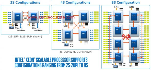
2S to 8S, Purley has you covered
As you can see from the red arrows the 2 UPI dies are equivalent to the older E5 2xxx and 4xxx series, the 3 UPI parts are E7 analogs. The fully connected bit is shown in the 4S configuration, the dotted arrows in the middle are 3 UPI fully connected parts, those without the third link are 2 UPI units with a 2-hop diameter in a 4S system.
Moving on to other interesting bits of platform trivia, the LBG blocks off the bottom are for Lewisburg, the chipset for Purley. This can be connected directly via DMI lanes or PCIe, or can be a standalone NIC/encryption engine. We won’t go into the details here but there is much more to Lewisburg than being a mere chipset for the Xeons, and there are multiple topologies that it can be used in. The simplest one is that each Xeon can have a Lewisburg attached or you can even have two Xeons directly connected to a single Lewisburg.
SemiAccurate thinks you will almost always see a single Lewisburg attached to a single Xeon for 2S configurations, but just remember you can do some rather silly things if you want. Some will, and if you see any in the wild, please email the author, after all curiosity leads to pointless knowledge. In the end the platform topologies for Purley can range from 1S to 8S with simple to very complex connection layouts.
To Die or not to Die:
As we previously mentioned there are three Skylake-SP die to choose from, the 28C XCC, the 18C HCC, and the 10C LCC, internally not code-named Papa Bear (PB), Mama Bear (MB) and Baby Bear (BB). That said they do prefer their porridge hot, warm, and cold respectively, something that should carry over to the 10nm parts as well. Seriously though here are the layouts for the smaller two dies.
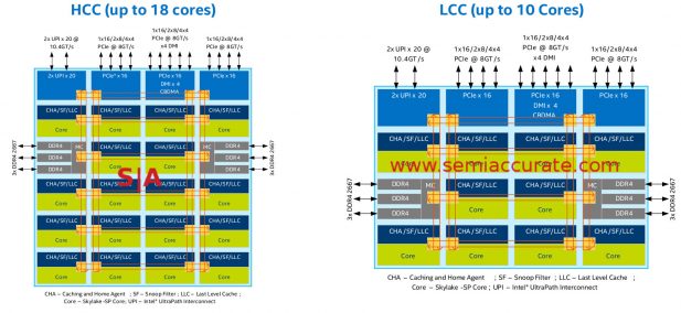
LCC is HCC minus 8
Lets start out with the easy ones, the HCC and LCC. Take an HCC and chop the lower eight cores off the bottom and voila, LCC. Other than that the two are the same. Both have 48 PCIe lanes across three root controllers, each can be implemented as 1×16, 2×8, or 4×4 lanes as you would expect. One of the controllers adds a 4x DMI link to it as well so connecting to a Lewisburg chipset via this channel does not eat any lanes from the main pool.
On the memory front there are the obligatory six channels, three on each side. They are situated in the middle of the chip, roughly speaking, for minimal latency. Also note that the I/O is clustered on the north, east, and west sides of the die, the south is completely free of I/0. This is a packaging concern but not a big one as the chips are out and they do work, motherboards are plentiful, and OEMs aren’t sniping in the background about it. One thing to note is that the UPI lanes have changed names and speeds, they used to be QPI and run at 9.6Gtps but now are at 10.4GTps. More importantly they now use PCIe3 signaling to talk so they should be a bit more efficient and more error tolerant. Unless you are designing boards this should be pretty academic.
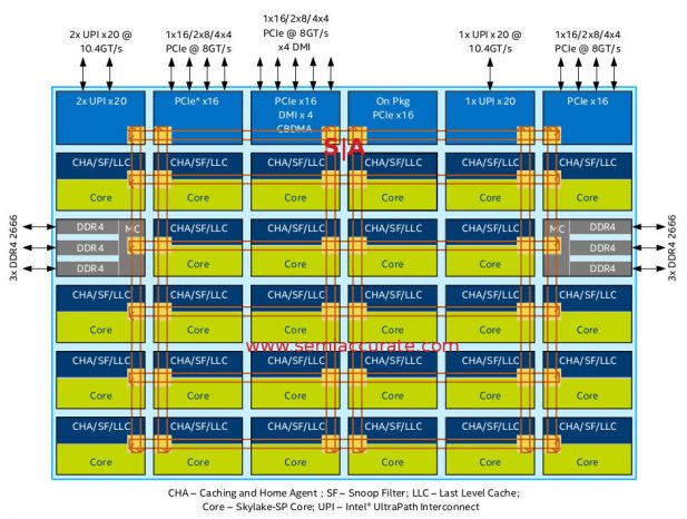
If you need 28 cores, you need XCC
The XCC die steps out from its smaller brethren in two ways both of which are columns. Core counts go to 28 and a second UPI block is added, HCC and LCC have one block that supports two 20x UPI links while the third block on XCC only supports one 20x UPI link but is otherwise functionally identical.
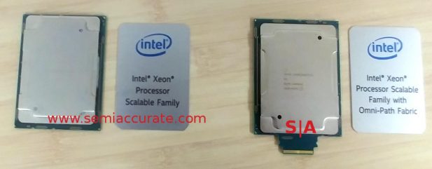
Stick your neck out for bandwidth
On the more interesting front is the block labeled “On Pkg PCIe x16”, and it does what it says. It is a fourth PCIe controller with PHYs for on package use, not off package. This is used to connect to the geoduck proboscis package extender that houses an Omnipath controller and someday an FPGA. There is also talk about putting and AI silicon and other bits from recent Intel acquisitions on the ‘neck’. Don’t take our cynical wording to imply that this isn’t a good idea, it is a great one. SemiAccurate thinks this is a clever hack by the Skylake-SP architects, well done.
One interesting thing to note is that these extra PCIe lanes are only on the XCC die, not the smaller HCC or LCC variants. That means that the -F suffix Onmipath bearing Xeons are all built from the big silicon die regardless of the core counts. This should also carry over to the FPGA and similar MCMs when they arrive.
On the more speculative front SemiAccurate has to wonder whether Intel will open this interface up to partners to add their own silicon as well. For a price. Our guess is that if you are big enough and by five or six digits worth of Xeons, units not price, a month, they would be happy to entertain such an offer. Again this is only speculation but for the right price, anything is usually possible.
A Meshy Situation:
Going back to the mesh interconnect which SemiAccurate covered in great detail about a month ago, there is an update. The diagram provided was simplified because Skylake-SP hadn’t launched yet. The main simplification was that the columns were equally spaced and laid out in an identical orientation. As you can see in the Skylake die diagrams above, they are actually not laid out that way but each core is mirrored allowing for a pairing of ring stops.
This seemingly minor difference has a big effect on latency. When going in the north-south direction, each hop has a one cycle latency on the mesh. In the east-west direction, hops from close stops (1 to 2, 3 to 4, and 5 to 6) have the same one cycle latency while going between long stops (2 to 3 and 5 to 6) have a three cycle latency. If you do the math this architecture shaves one cycle from a worst case east-west traverse over a hypothetical even 2 cycle hop latency part. This also falls under the category of clever hacks, all that work to shave a single cycle of latency but that is where speed and energy savings come from now, details. Intel obviously sweated them here.
Cluster Tricks:
One last new trick is something between a platform feature and a chip feature but we will lump Sub-NUMA Cluster (SNC) in with the platform features. The idea is similar to the older Cluster-On-Die feature of previous Xeon families but a bit more advanced. As the name suggests you can split up a Skylake-SP die into two logical entities and cluster them like a 2S system.
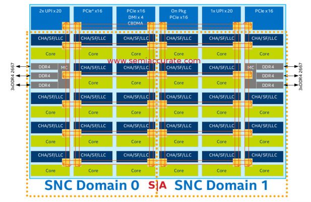
SNC is the new CoD
Why would you do this? To save bandwidth, power, and latency mainly, but there is also the possibility of lockstep type operation although we are not sure that is available in this configuration. The idea is to take half the cores and logically split them off from the other half. This of course halves the ‘local’ resources for each core but it also halves the users for each ‘local’ resource.
The result is the L3 cache only has to keep track of the data from half the cores, but it is half as large. Memory bandwidth is halved but again it has half the cores to support. If this all seems like a net equal trade it isn’t for one reason, traffic. Coherency data goes up more than linearly with core count and a memory request has a 6 hop worst case distance with SNC vs 12 hops without SNC. Also all these memory requests to controllers and PCIe resources on the far side of the die cross and therefore block far fewer nodes.
The net result is far less than half the traffic is generated on the mesh. This obviously means less contention for resources, less delays, and as with real world traffic, things are better when there is no congestion. More importantly is that pushing all these high-speed signals across the die is expensive, it takes a lot of energy. By significantly decreasing the worst case, and average case hop distance to any given resource, you save tons of energy. Any time you can save energy in a modern CPU you can usually use that in other ways, most notably by upping clocks a bit more. SNC can be a significant win for some types of workloads.
But what happens if you need more of the resources than SNC delivers, say memory bandwidth or PCIe lanes? The simple answer is to not use SNC mode but that would be too easy. If you are in SNC mode and need to use something on the remote memory controller, you can, it is that easy. Why? Remember the C in SNC stands for Cluster. One half of the SNC cluster can access the far memory controller just like you could access a memory controller in a far socket via a UPI link, but in this case you don’t pay the massive latency penalty. In short those far resources are still available if needed but by minimizing their use the net gain is pretty huge and the penalty can be minimal. As with most things the results will vary with your workload.
Overall:
With Skylake-SP and the Purley platform, Intel has simplified some things and made others more complex. On a technical level the architecture is much more advanced, a single platform now scales from 1S to 8S and has options for integrated co-processors, direct fabric connections, and more in the future. Memory channels have gone up from four to six, and the internal mesh is far superior to the older multi-ring topology. All in all Purley is a solid step forward from Grantley with room to grow in the future.S|A
Charlie Demerjian
Latest posts by Charlie Demerjian (see all)
- Nuvia Founders Have A New Startup, Nuvacore - Apr 16, 2026
- Nvidia Is Negotiating To Buy A Large PC Oriented Company - Apr 13, 2026
- Dell Does Modular Laptop Boards Right - Apr 7, 2026
- Qualcomm Snapdragon X2 Review Embargo Lifts Tomorrow Morning - Apr 6, 2026
- Intel Cuts HDR OLED Panel Power with SmartHDR - Apr 2, 2026