 Intel’s Skylake-SP Xeon’s aren’t the same core as the consumer versions, divergence is real. That potentially makes it one of the most interesting cores SemiAccurate has seen in a long time even if Intel won’t let us actually see it.
Two cores to rule them all:
You might remember the dark days of 2014 when SemiAccurate told you about Intel and core convergence. If consumer cores converge that probably means server cores will diverge, or at least that is what SemiAccurate speculated. Guess what? The new Xeon core is not the same as the desktop core, or at least it isn’t for the XCC die based Platinum 81xx and Gold 61xx Xeons. That said the Gold 51xx, Silver 41xx, and Bronze 31xx cores are the same as your gamer and consumer cores.
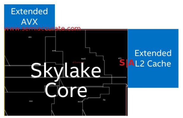
Skylake-SP’s core extensions
The changes are threefold, AVX, L2 cache, and L1-D bandwidth. Starting out with the easy ones we have the L2 cache which grows by 768KB but does so ‘outside’ of the core. This means the cache is tacked on the periphery of the core itself meaning Intel had to prepare for it architecturally in the consumer parts. Unfortunately Intel no longer releases die shots or transistor counts, more on this later, so we can’t show you the nifty things they say they have done. Same with the L1-D bandwidth which doubles to support 2x64B, not b, loads and 1x64B store per cycle. Why? Funny you should ask because….
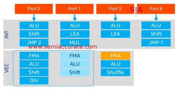
Porting new AVX-512 units
Because of the third new feature, the second AVX-512 unit. Before you wonder what we are smoking, yes Skylake the lesser, aka the non-SP consumer versions had two AVX units as well so what is the fuss about? They had AVX-512 APIs and could process AVX-512 code but the physical units, ports 0 and 1, were each only 256b wide. A full width AVX-512 instruction took two cycles or more to complete because it needed to be done in two passes. Those two 256b wide units are now fused into a single physically 512b wide unit and Port 5 now is also AVX-512 with full physical width.
This new unit, and it is pretty big, has been added ‘outside’ the core. Again pictures or it didn’t happen, and Intel is not improving their image or trustworthiness with the lack of information. That said if the units are actually done in a modular fashion like Intel claims, it is an incredible technical achievement. Given Intel’s reticence to talk about all things transistors and other things, we have reason to doubt they actually did what they claim. Until they offer real proof, keep an open mind on this one.
Speed Daemons, Cores, and Meshes:
Next up is speed or lack thereof. In this case lacking speed is mostly a good thing because it saves power. The cores obviously clock down and turbo when needed and so does the mesh. For the higher end SKUs the mesh usually runs between 1.8-2.4GHz as demand necessitates. Given the wording of the explanation, it sounds like those aren’t hard limits but common working ranges instead. Given what the mesh does, and how, it is probably a safe bet that those frequencies aren’t exceeded very often up or down.
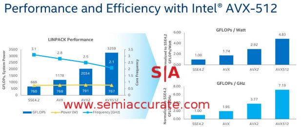
AVX clocks slide in this slide
One hot topic among the enthusiasts is Intel’s AVX clock, a widely misunderstood feature. What it does is quite simple, when the system detects more than a certain number of AVX instructions per time unit, it drops the clock of the core. Without AVX it runs at normal clocks IE 3.1GHz top turbo on the 8180. AVX drops that top clock 300Mz to 2.8GHz, AVX2 drops it another 300MHz to 2.5GHz, and AVX-512 hammers things down 400MHz more to 2.1GHz top speed or 400MHz below the base clock.
At this point most enthusiasts tend to start the conspiracy laden forum posts about how awful AVXx is because of the clock drop, and then the frothing at the mouth begins. In reality the AVX clock drops are a good thing, sort of, because they allow so much more work to be done. If your code does not use AVXx instructions it won’t trigger the speed hit, if it does you get significantly more performance at the same net energy usage. The sort of qualifier earlier is simply there because if Intel could make the clocks not drop it would be better yet, but since they can’t you are still better off with wider but slower vector instructions. SemiAccurate has previously published some theories about why AVX clocks are necessary, make of them what you will.
Cache cachet:
Moving back to caches there is one more interesting change other than the L2 going from 256K to 1MB and the L3 dropping from 2.5MB to 1.375MB. That change is the caches go from inclusive to exclusive. Why? As core counts climb inclusive caches need to mirror the contents of each L2 and although they are big enough to do so on previous architectures like Broadwell-EP/EX, you end up putting more and more cache down just to keep up. 24 Broadwell cores means 6MB of the L3 is eaten up by data in the L2 and if you did the same with Skylake-SP you would chew up 28MB of L3, assuming the L2 gains still happened. Think of this as a rebalancing of the cache hierarchy with the tipping point in the 25-28 core range.
That brings us to another problem, coherency and coherency traffic. In previous architectures coherency was handled at the memory controller and home agents. If you flip back and forth between the block diagrams of Broadwell and Skylake you might notice there are no home agent (HA) blocks this time around either. Both the HA and the coherency logic are rolled into one unit now called the Caching Home Agent (CHA) and are distributed with each LLC slice. This obviously eliminates traffic between the HAs and memory controllers and Intel claims it will now allow snoops to be launched earlier. Intel claims the result is far lower L2 misses and more or less the same L3 miss rate but overall it is a big win. Also not having to put down MBs of cache doesn’t hurt margins either.
Proxy that PCIe:
Next up is an unexpected feature Intel calls VMD or Volume Management Device, a controller for each PCIe domain. Every VMD manages 16x PCIe lanes and can be turned on or off in the BIOS with a 4-lane granularity. What VMD does is effectively proxy the PCIe lanes so the host CPUs and OS see a single VMD instantiation instead of raw PCIe lanes. This allows the VMD to aggregate the lanes into a transparent RAID for example. PCIe RAID is a tricky thing at the best of times and VMD seems like a sane way to make it happen until the various standards bodies catch up. PCIe storage is the (really near) future so we think VMD is a very good thing.
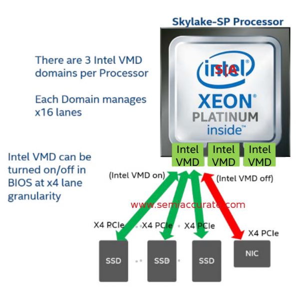
Think shims not devices
One other important bit is that PCIe is notoriously twitchy, a single error can hang a full server with little recourse from the hardware. There are various ways to insulate a hung PCIe device from doing the same to the system, PLX has one very elegant solution, but the problem is very nasty. Insert Windows stability joke here just for added laughs. That said VMD has the potential to stop this class of system hangs by proxying the PCIe lanes, as long as the VMD controller doesn’t hang, the system should be insulated from hung devices. It also seems like a nice start for some very slick hot plug capabilities.
Self-Inflicted Wounds:
You might have noticed that SemiAccurate, or anyone else, didn’t publish a die shot or transistor counts. We did ask. Intel replied, “… on die shots, wafer shots & transistor counts, Intel is no longer providing this information. Within TMG and DCG, we consider this information proprietary to Intel’s business operation.” The first thing you wonder about is why the change. Intel has unquestionably lost the lead in process technology and is going out of their way to hide it, but that doesn’t answer the question. There are three answers here, pick the one you think is most reasonable.
First is the good spin, Intel is way ahead of the competition, the dies are much smaller, and they are better at everything than the pretenders snapping at their ankles. If this is true all they are doing is not telling the world, unwashed and stockholders, about their advantages. It is both silly and a self-inflicted wound, no gain but lots of pain.
Second up is their counter to die shots, and it is the middle ground scenario. At times Intel claims the pictures will reveal secrets or something similar to the competition. This is farcical because if you look at process tech, by the time the devices are out, the competition has their similar geometry processes either out or fixed by that point. Anything learned by a low-rez press picture won’t help and even if it did, by the time it can be applied, the process in question is out of date and those techniques don’t apply to +1 or +2 nodes. Besides that any serious competitor will have purchased the product in question months ago and had it professionally torn down revealing much more detail. There is no chance that ‘trade secrets’ will leak from press pictures, but that story does sound nice to the technically illiterate, nevermind a 30+ year history of releasing such images.
The last option is the least happy spin, namely that the die is much bigger than Intel wants it to be. Since die size is one of the major contributors to a device’s cost, it matters a lot. Skylake-SP is late and slipping, the fully debugged Purley is now called Cascade Lake and will come some time next year. Silicon ages about as well as fish and Purley is getting quite ripe. Age also equates to performance, the later a project is, the higher it has to perform to keep up with expectations. This too has a bearing on ASPs, just ask AMD of old about how well some of their late server chips fared in the market.
So Intel not disclosing die sizes and transistor counts STRONGLY suggests that Skylake-SP is far bigger than they would like it to be. It is on the same 14nm process as the older Broadwell-EP/EX and core for core only outperforms it by about 10%. Add in four more cores and you get another ~15% bump. That should put some bounds on costs vs Broadwell but without the die sizes it is hard to tell if Skylake-SP is above or below water here. Investors, start your engines.
Either way Intel’s refusal to put out basic information that all their competition puts out is a self-inflicted wound. It raises some very uncomfortable questions about where they actually stand. If they are hiding a bloated die, what else are they hiding? In any case there is no up side to this non-disclosure, the information will be out soon enough from third parties and Intel cannot control that. What is the point of blackening their own eye?
Details, Details:
There are a lot more minor changes to the Skylake-SP architecture from internal buffers to registers. Each adds not only a fraction of a percent performance but usually a bit more in efficiency. It all adds up to the claimed 10% higher integer performance Intel has claimed for Skylake overall. On the consumer side the numbers often go much higher due to GPU increases being rolled in and AVX-512 has the same effect on server parts. That said realistically you should expect small gains from most code over Broadwell-EP/EX, more if your code is amenable to AVX-512 and you recompile, but slightly larger efficiency gains.
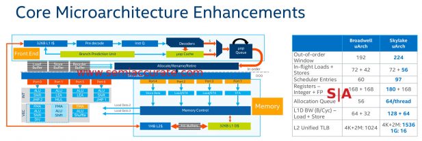
Details really do add up
On top of this there are some nifty tricks Intel seems to have pulled off with AVX-512 that were mentioned in the Skylake-SP briefing but were really covered in a briefing that SemiAccurate wasn’t invited to months earlier. Because of this we can’t accurately comment on the advances we will point you, if you are curious, to the software optimization manuals cover it in great detail, enjoy.
Core Conclusions:
Other than that the Skylake-SP core is about what you would expect, a little more performance than Broadwell-EP/EX for a little less power. There are some serious potentially innovative areas like the new AVX-512 unit and the added cache but without die shots and more disclosures, they only look innovative on paper. Some have suggested the added units have been there all along, other deny it, and Intel refuses to clarify.
Skylake-SP is out now but several key elements of the platform are still missing. That list includes FPGAs on package, Xpoint/Apache Pass support, and a host of other minor features which are now officially slated for Cascade Lake. A year ago all of these were slated for a mid-Q2 release and now they are due next year. That said the Skylake-SP core is finally here and it does move the needle in the right direction but doesn’t change the game.S|A
Charlie Demerjian
Latest posts by Charlie Demerjian (see all)
- Nuvia Founders Have A New Startup, Nuvacore - Apr 16, 2026
- Nvidia Is Negotiating To Buy A Large PC Oriented Company - Apr 13, 2026
- Dell Does Modular Laptop Boards Right - Apr 7, 2026
- Qualcomm Snapdragon X2 Review Embargo Lifts Tomorrow Morning - Apr 6, 2026
- Intel Cuts HDR OLED Panel Power with SmartHDR - Apr 2, 2026