 It has been a long time since SemiAccurate used a CPU that felt significantly faster than the last one. AMD’s Ryzen 5000 line with their new Zen 3 core did just that.
Preface:
Lets start out our look at the AMD Ryzen 5000 CPUs by saying we are getting back in to testing after a long absence and there are a lot of teething problems, things that are missing, and much to relearn. We only had a short time to play with a fully working Ryzen 5950 system but it impressed us. The boot speed of Linux Mint 20 was so fast it was noticeable, literally a fraction of the time it takes on our main daily system. Much of this is down to the PCIe4 SSD but the CPUs have to process that data when it comes in.
Within a few minutes of fooling around on the system, an AMD Ryzen 9 5950X on an Gigabyte X570 Aorus Master with a Samsung 980 Pro PCIe4 SSD and 16GB of GSkill Trident Z Royal DDR4-3600 memory the system was running at 4.5GHz on all cores at 1.25v. Not bad. Jacking the memory up to DDR4-4000 reliably booted to desktop but crashed a few hours into the benchmark run so no numbers until we have time to relearn a lot of things.
With all that in mind there is one thing that stands out too us, this system is seriously fast. Since it is the highest end gaming PC on the market right now, you would expect it to post the best numbers, and a brief glance around the net shows it does live up to SemiAccurate’s earlier claim that “AMD should win at everything now and Intel has no response“. The only real question is how it gets there, and that is a long story.
At a High Level:
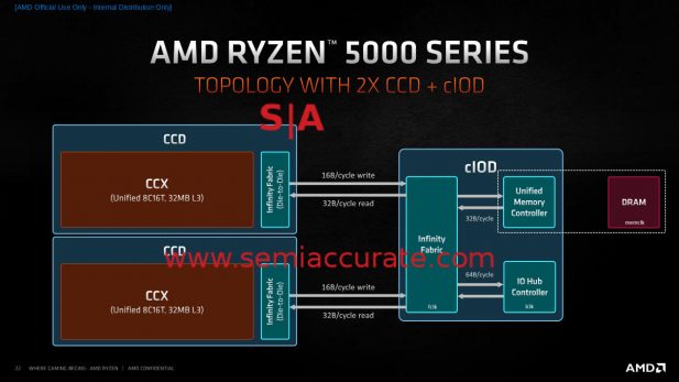
Ryzen 5000 Chiplet Layout
If you look at a high level block diagram of The Ryzen 5000 CPUs, they look like the Zen 2 based Ryzen 3000 devices. There are one or two CCDs, built on an evolved 7nm process (+ or ++ in Intel-speak), and one cIOD. That cIOD is the exact same chip as the cIOD in the R3K line, literally nothing has changed on this 125mm^2, 2.09 billion transistor 12nm die from Global Foundries.
On the CCD side, just about everything changed, but for now we will focus on the die itself. Those changes necessitated a new package, the wiring isn’t the same, but nothing much more than that. Each CCD is 80.7mm^2 and contains 4.15 billion transistors. This means the total silicon area is 205.7mm^2 for the single CCD packages, 286.4mm^2 for the 2 CCD SKUs. More impressive is that AMD was able to up the memory speeds supported to DDR4-4000 without changing the cIOD which contains the memory controller. This has some very interesting implications for the Milan based server products, but that is a story for another day.
More Cache:
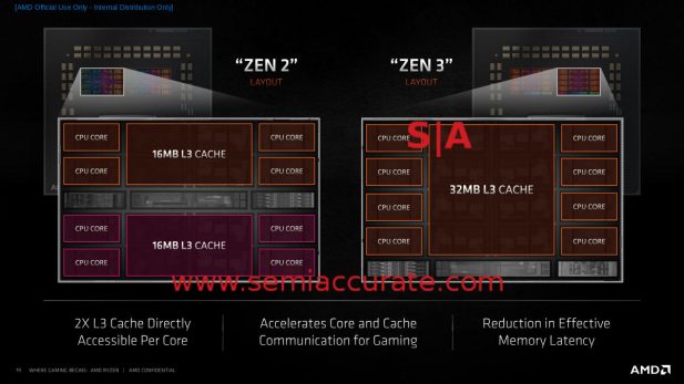
Delving into the CCD a little deeper we see some differences emerge, specifically at the core organization level. Zen 2/Rome CCDs were logically subdivided into two 4C CCXs, each with 16MB of L3 cache. Those two cache slices and core clusters were not directly connected, for core 4 to talk to core 5, it had to leave the die, go to the cOID, and then back out to the other CCX on the same CCD. This was a tremendous waste of energy, added latency, and in general wasn’t a good idea. About the only good thing you could say is that the latency between any two CCXs was fairly consistent.
Zen 2 vs Zen 3 CCX arrangement
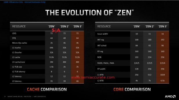
Zen 3/Milan however fixes this by upping the CCX to 8C with 32MB of directly accessible L3 cache. Each L3 cache piece is address sliced but going to the other CCD still means a few package and cIOD traversals, and the links are far less loaded than they were on Zen 2 devices. With a little OS scheduler support or software optimization, this should result in significantly better overall performance. On the down side the larger L3 means that latency went from 39 cycles in the 16MB Zen 2 L3 to 46 cycles in Ryzen 5000. Overall worst case is a little worse but average and real world performance is significantly better and that shows in the numbers coming out at launch.
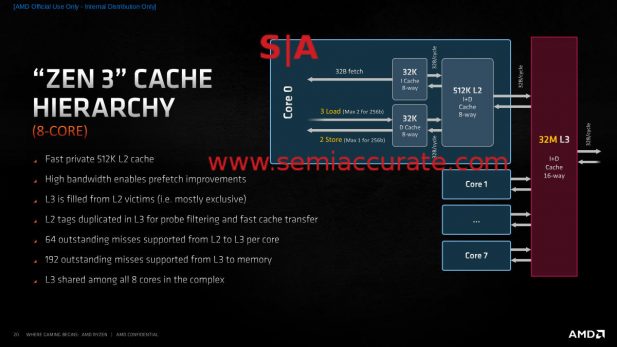
Zen 3 Cache Hierarchy
Moving on the the L1 and L2 caches, not much has fundamentally changed from the last generation. L1 I$ and D$ are still 32k each and the L2 remains at 512K, latency is unchanged on all three. The L3 is a victim cache so it only gets filled when things are evicted from the L2 but it has shadow tags so other cores can pull from L2s on the same die without going off-die to the memory controller.
You will be referring to this a bit
Bandwidth is also improved starting at the core which can now do three loads or two stores per cycle unless it is a 256b operation which maxes out at two and one respectively. The path to memory is 32B/cycle all the way with the exception of L3 writes to memory which are only 16B/cycle. Other than that not much has changed as you can see from the table above. Everything is either the same or a little better and the dividends show in real world workloads.
Into the Core:
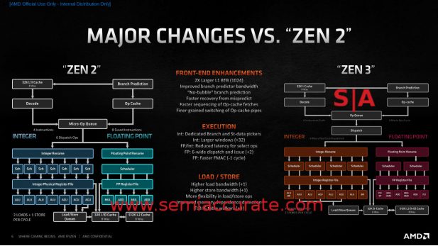
In case you haven’t heard by now the Zen 3 core is all new. A few features were pulled in to the Zen 2 core because they could, but this device it is not evolutionary. Integer pipes go from 7 to 10, FP from 4 to 6, and everything is claimed to be better utilized. AMD described the goals of the new core as performance, latency, and efficiency. Net energy use didn’t go up, IPC increased by 19%, and performance per Watt rises by a claimed 24%, all of which seem to indicate that AMD hit their goals.
Zen 2 vs Zen 3 Block Diagrams
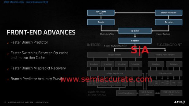
As always the devil is in the details but even from a high level point of view it is clear that a lot has changed internally. On the front end, things look fairly similar between the two architectures but Zen 3 split the Micro-Op Queue into Op Queue and Dispatch stages, but the real differences are more nuanced. The BTB doubled, branch predictor bandwidth increased, latency went down, accuracy went up, and transitions are better handled.
Zen 3 Front End Overview
The branch predictor getting faster is nice, as is a slight increase in accuracy, but the big win is in latency. The ‘no bubble’ claim means that once something is predicted, that result can be used on the next cycle instead of having to wait while it is sent to the right block. This is really hard to do and AMD would not comment on exact methods but it takes a large chunk out of latency. Similarly the time it takes to recover from a mispredict is also reduced, again for lower predict latency.
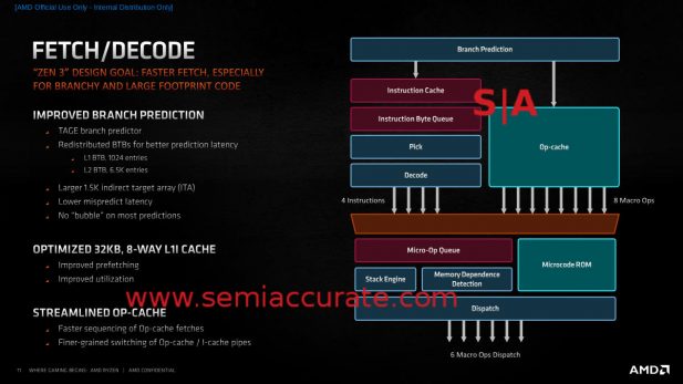
Zen 3’s Fetch/Decode Unit
The branch predictor feeds the I$ and once there, four ops can be pulled into the queue per cycle. AMD improved how corner cases and boundary transitions are handled which again improves latency. That said the x86 variable length operands are a pain and even with the improvements things can get complex fast. Once decoded and stored in the Op-Cache, those boundaries are known and things are a lot saner so eight ops per cycle can be dispatched to that orange box without a name.
Said semi-anonymous orange box is important because one headache with Zen 2 was re-combining ops from the I$ side and the Op-Cache side, it could take a little bit to line everything up correctly. Zen 3 does this a lot faster which once again takes a chunk out of latency and once again is proprietary. On top of this the decisions made by this unit are a lot finer grained so a little better, a little faster. All in all this adds up to a slightly more accurate front end with a lot lower latency, a huge win on performance and power.
Integers Go Up:
The front end of Zen 3 can issue 16 instructions per cycle up from 11 in Zen 2. In an almost magical coincidence that number is pretty close to the 16 pipes that Zen 3 has, up from 11 in Zen 2. The Int side of the house now has 10 pipes, up from 7, and the FP side has 6 up from 4. Wider is better as long as it can be fed properly and doesn’t blow out your power budget like earlier wide architectures tended to do. As you can see from the overall chip’s efficiency, AMD seems to have balanced things right on this front.
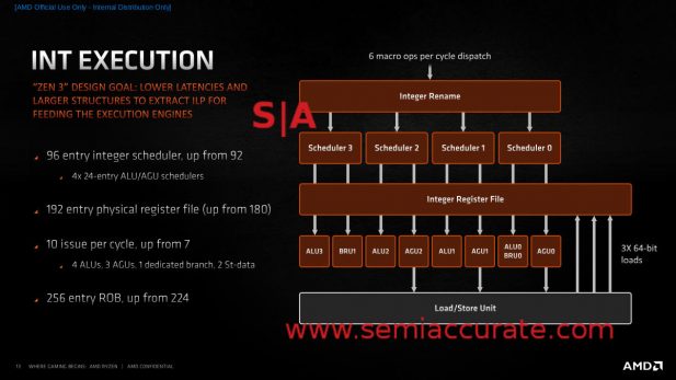
Zen 3’s Integer Unit
The scheduler went up from 92 to 96 entries, more specifically four 24-entry schedulers as you can see from the diagram above, the physical register file goes up 12 to 192 and the ROB is 256 entry instead of Zen 2’s 224. Those numbers are useful on the efficiency front and make sure every unit has enough to keep things optimally fed, but the real change is in the pipes themselves.
As you can see there are now 4 ALUs, 3 AGUs, a dedicated branch unit, and 2 store units. Each of these 10 units (Note not all are pictured in the slide above) can be fed every cycle which is a big improvement from Zen 2. Also note that the pipes are arranged so each ALU/AGU pair is fed by one scheduler but they are still able to work independently. This is a big part of the efficiency, it allows for more work with less complexity. If you had to summarize it, pipes were added to avoid contention and they are arranged better for similar reasons. Less complexity and wiring tends to make things more efficient, and that is the point.
FP Unit ver. 3.000000:
Add 2.00000 FP Pipes
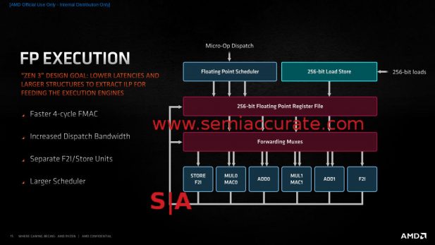
On the FP side latency was a key optimization area as well, as is wider issue. There are still 2 Mul and 2 Add pipes, but the F2I (Float 2 Integer) functions have been broken out to separate pipes and one is combined with a store unit. This obviously lowers contention and since all six pipes can be fed at once, it improves throughput. One cycle has been shaved off Zen 2’s 5-cycle FMAC operation so latency goes down here too. The scheduler grows a bit as does internal bandwidth, so all is well there. Additionally the elves that lift the numbers up to the exponent have more comfy chairs to sit in when the FP unit is idle so they will be fresh when needed. Just checking to see if you are still paying attention.
Loading and Storing:
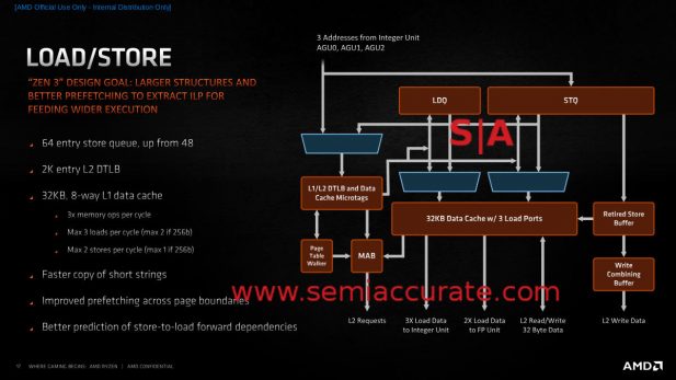
Load/Store is always a fun topic to discuss with non-technical friends and AMD gives us some new things to bring up this time around. The main one is the 3 AGUs now mean they can do three loads per cycle or two stores or two and one if they are 256b values as mentioned earlier. This is a double win, more bandwidth and more flexibility, a rare thing in modern hyper-optimized cores. There is also better memory dependence detection and four more TLB walkers for a total of six.
Instead of Football, Discuss This at the Bar
The rest of the improvements can be summed up as, “things got better everywhere”. The store queue went up by 33% to 64-entry but the raw sizes of most other structures are more or less the same. Better prefetch across page boundaries was called out earlier and there is also better prediction of store-to-load forward dependencies. One instruction that was specifically called out was REP MOVSB which had really high latency for short copies. In Zen 3 that was reduced a lot on short iteration counts, improved on mid-counts, and still workes OK on long runs. Again, a little latency reduction in many areas pays big dividends and that is what changes to the Load/Store unit are all about.
Odds and Ends:
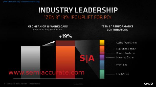
There are a lot of other little things that once again add up to make the Zen 3 core faster and more efficient than Zen 2. Several instructions execute faster, some of which were noted above, and a lot of things like the instruction sequencing when going between Op caches have far lower latency. These all add up to big numbers in the end, specifically the 19% IPC increase AMD claims and the 24% performance per Watt uplift.
IPC Broken Down by Color
On top of this there are a few new features, some minor, some significant. On the security side, Zen 3 now supports Control-Flow Enforcement Technology (CET), basically a shadow stack to stop ROP attacks. Two instructions, VAES and VPCLMULQD, now have AVX2 support which should be a big relief to the throngs of fans waiting for this to happen. Even more throngs of fans are awaiting AMD’s description of MPK which effectively allows more granular memory permissions. SemiAccurate asked about it, AMD didn’t explain but we think they will really soon when Milan/Epyc 3 is revealed.
AMD does disclosure right
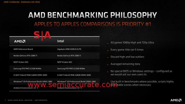
Another good thing is AMD finally did some solid disclosure on their benchmarking setup. If this continues, SemiAccurate will finally be able to both accept the numbers they present and stop bitching. See, it wasn’t that hard to do the right thing, and hopefully the GPU side will get on the train soon too. Whatever the outcome, recreatable numbers are mandatory for trust and the Zen 3 decks show both sides can do right and still make the claims they need to.
Conclusion:
In the end we are here, Zen 3 in the form of the Ryzen 5000 family is out and from afar it looks pretty much like Zen 2/Ryzen 3000. Once you zoom in you can see that everything on the CCD is new from the ground up. The 19% IPC uplift means that AMD wins at everything now, all the former Intel strongholds and significant corner cases are now clear Ryzen wins. Yes there are a few things here and there where Intel can still take a the odd win but it is just that, the odd win. When AMD priced their products above Intel, you knew it was over.
From here we expect the 5nm Zen 4 to hit the shelves in just over a year, lets call it early 2022, and bring substantial performance benefits. Between now and then Intel has nothing to counter AMD with, the 10nm parts that can’t be made and 14nm parts that aren’t in the same ballpark. Zen 3 has a clear run for the next year, the fact that it is so good is icing on the cake. As we said earlier, AMD wins at just about everything.S|A
Charlie Demerjian
Latest posts by Charlie Demerjian (see all)
- Nuvia Founders Have A New Startup, Nuvacore - Apr 16, 2026
- Nvidia Is Negotiating To Buy A Large PC Oriented Company - Apr 13, 2026
- Dell Does Modular Laptop Boards Right - Apr 7, 2026
- Qualcomm Snapdragon X2 Review Embargo Lifts Tomorrow Morning - Apr 6, 2026
- Intel Cuts HDR OLED Panel Power with SmartHDR - Apr 2, 2026
