 Today AMD launches their new Ryzen 5000 mobile line of CPUs based (mostly) on the Zen 3 core. The important bits were teased by AMD weeks ago so SemiAccurate will just give you a bunch of interesting details.
The main parts of AMD’s Ryzen 5000 mobile/APU (R5KM) are well known because they are already out in different forms. Zen 3 cores are on the market in the Ryzen 5000 non-mobile line on the CCD chiplet in those CPUs. In APU guise there are a few differences, mainly that the core complex is a unified 16MB L3 cache instead of 2x4MB in the Zen 2 models, both half the cache of their server/HEDT brethren.
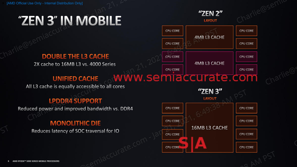
Half the cache, all the cores
Note the bottom right
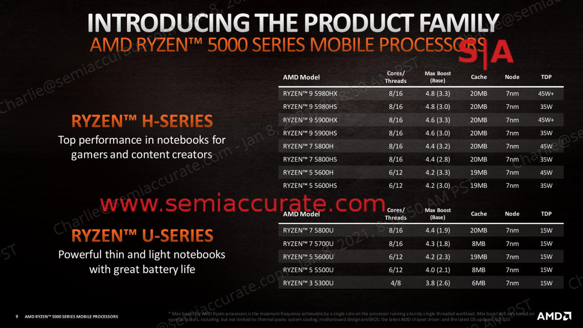
Things get interesting when you dive a little deeper under the hood though. If you look at the U-Series in the table above, you will see that three of the five, 5700U, 5500U, and 5300U, are all Zen 2 based rather than the expected Zen 3 cores. This means half the cache, the old core architecture, and more. Luckily for AMD those cores are pretty good, market leading in most ways so their inclusion, or at least not having Zen 3 based SoCs for those parts, isn’t the end of the world.
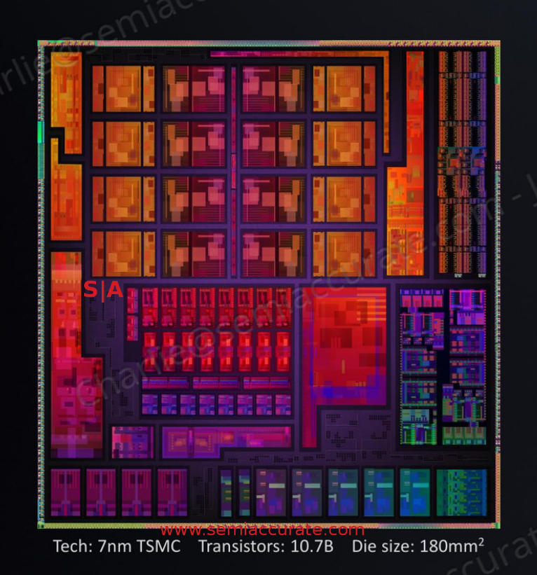
Obligatory pretty die shot
So why do it? Why regress especially since the rest of the SoC is exactly the same as Zen 3 parts? Money, or at least cost which seems a bit counter-intuitive since AMD has to design, tape out, and validate a second die for just three SKUs. That answer lies in the bottom of the image above, the part that reads 180mm and 10.7B transistors. The Zen 2 SKUs are on the same process but take up 156mm and 9.8B transistors, roughly a 10% die area savings. Most of this is accounted for by having 8MB less L3 cache but the cores are a bit smaller as well.
![]()
Buy These Versions
AMD claims the OEMs were very price sensitive and that margin matters so Zen 2 to the rescue. Since AMD is severely capacity bound at the moment, a 10% savings on area for higher volume SKUs is welcome too. AMD says they will put a holographic sticker on all Zen 3 models to differentiate them, something SemiAccurate welcomes. The gaming oriented SoCs, basically the 35/45/45+W models, will all be Zen 3 based.
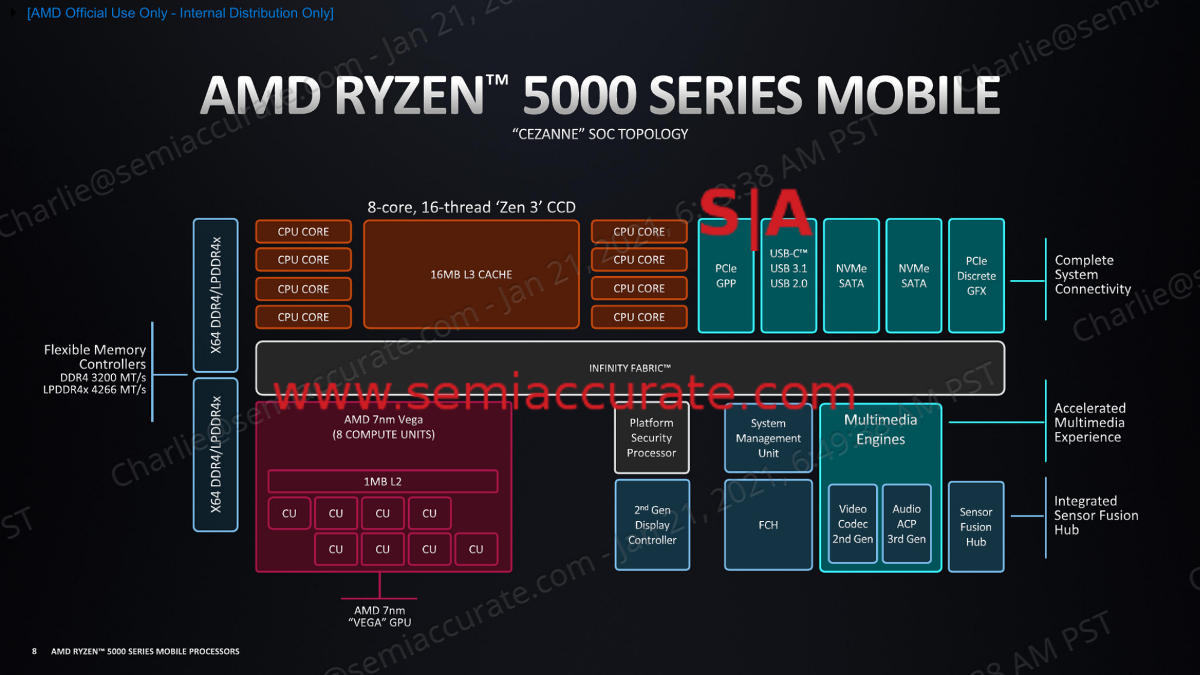
Obligatory block diagram
One very interesting detail is the CCX <-> Infinity Fabric connection. You might recall in the larger/non-APU Ryzen desktop parts, the CCD chiplets were connected to the IOD chiplet with a 32b wide read, 16b wide write per cycle bus. On the APUs, this is increased to 32b/32b R/W for both the Zen 2 and Zen 3 based SoCs, the 2x4C layout doesn’t affect the connections to the fabric. You can probably win bets at a bar with this, we won’t ask for a percentage if you do.
On the memory side, the R5KM line add two features, power savings and LPDDR4x. The power savings are based on a deep power state for the memory controller and AMD claims it will enter in lower activity workloads and come out ‘fast’. During this state the PHYs are placed on a lower voltage rail and so uses less energy. This is the table stakes for exploiting LPDDR4x which is now supported to 4266 MTps speeds. Better yet you can buy chips that are double the density of vanilla DDR4 so hopefully we will see laptops with increased capacity rather than one channel with the same capacity to save a few cents.
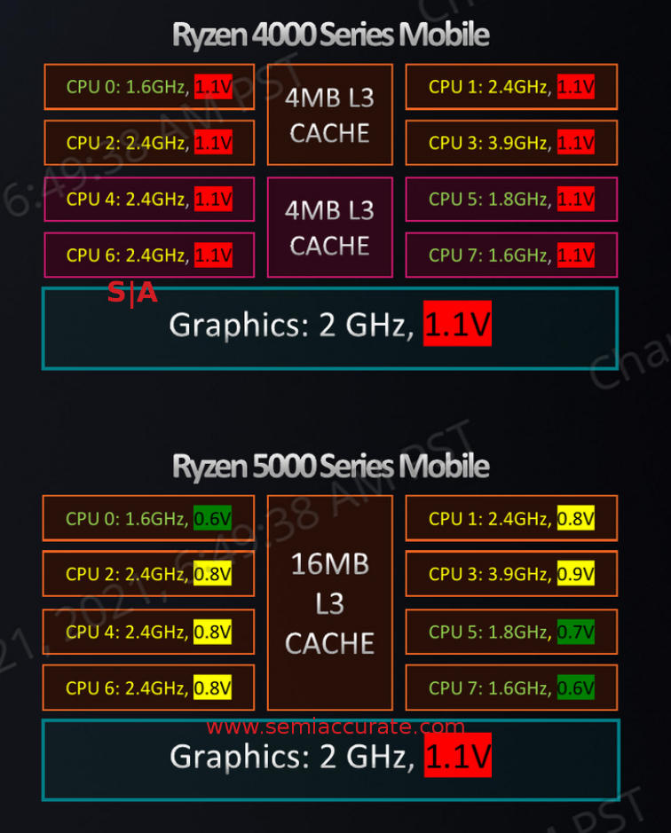
This is the big bang on energy use
Speaking of lower power, AMD has now enabled CPPC or Collaborative Processor Performance Control on R5KM. This closed loop power savings methodology has been with us for several generations in desktop form but this is the first implementation (Activation?) in mobile. While interesting on it’s own, coupling CPPC with per-core on die voltage regulation via DLDOs as you can see above, is worth a lot more than either option alone. The GPU is on it’s own voltage plane too but now the entire system is not tied to that state as it was in R4KM. This should result in substantial energy savings.
The rest of the SoC is pretty much the same as the R4K line, the only real addition SemiAccurate can find is Control-Flow Enforcement Technology (CET) on the Zen 3 cored models. There are tweaks to the GPU to allow for throttling down in bandwidth constrained situations like the Radeon 6000, something that may be tied to the new memory controller power awareness. In any case the rest of the system is pretty much as the R4KM was, PCIe3, same IO, and all the rest. This isn’t bad but PCIe3 is getting crusty, Intel will destroy this part is storage benchmarks as a result, and that performance matters to the author.
The up side is that R5KM is pin compatible with R4KM, all the power goodies are on-die so they ‘just work’ even in carryover designs. This should mean a lot faster launch of new models, something we are seeing in the market already, and cost savings to the OEMs who can extend the life of their sunk engineering costs for those models. If you wanted to take the optimistic view, you could say that the money that would have been used to redo the boards can now be used to make specialty devices like bespoke gaming chassis and other related things. So far the R5K is off to a solid start.S|A
Charlie Demerjian
Latest posts by Charlie Demerjian (see all)
- Intel Bumps Xeon Memory Speeds - Jul 20, 2026
- Qualcomm’s 2026 Investor Day Has Hidden Goodies - Jul 15, 2026
- Phison Phudges The Numbers… In A Good Way - Jun 24, 2026
- Who Are The Qualcomm Enterprise Customers? - Jun 23, 2026
- Innodisk Adds 10GbE To Useless M.2 Slots - Jun 19, 2026