![]() Intel held an Architecture Day recently with 11 topics covered from cores to software and more. SemiAccurate wasn’t able to get the basic information needed to cover any of these topics so we will just puke out a few interesting bits.
Intel held an Architecture Day recently with 11 topics covered from cores to software and more. SemiAccurate wasn’t able to get the basic information needed to cover any of these topics so we will just puke out a few interesting bits.
Authors Note: The Architecture Day was the third in a series of events that promised deep technical dives into the details of products being discussed. The first one was just that covering things like Foveros, Lakefield, OneAPI/Software, and much more. It was a full day on 2-3 main topics with ample time to discuss things with the relevant engineers, see demos, and ask questions. The time until the embargo lift was short but mostly workable. The second event was less technical, more topics, and from memory a shorter embargo lift time.
This year Intel promised an architectural deep dive into several topics with all the depth and details you could possibly use, and they delivered. Unfortunately we are not a YouTube channel that focuses on makeup tips for lower education markets, instead we write about tech. In that light, Architecture Day essentially had none. There were 11 major topics covered in 2:20. Take out a bit of time for the various intros, videos, and transitions and you are looking at less than 10 minutes per topic. If that sounds OK, bear in mind we are talking things like new core architectures, new SoC load balancing paradigms, and so on. In previous years, these topics would have been 1-2 days each, plus two weeks to ask questions about them and get answers back.
After the initial briefs there were ~3 hours of Q&A time the next day, then less than a day until all 11 stories had their embargos lift. There literally wasn’t enough time to get the initial round of questions answered much less write anything cogent on them. After the initial briefings SemiAccurate sent a list of 89 first round questions to Intel just to get the basic info we needed to understand the topics, mostly things that should have been covered as table stakes in the brief. At this point we have to say the front line PR people went above and beyond the call of duty to try and get the answers and support the press but they had the same constraints we did, plus they were getting flack from above and below on things they had no control over like topics, timing, and schedules. They are likely to get the blame for the whole fiasco too even though they are just doing what they were tasked to do. Blame the messenger, not the bosses.
Back to the point, to compound the problem, the Architecture Day lacked one big thing, architecture. Not joking here, that YouTube makeup channel crack was serious, there was almost no tech in tech day. The format of the talks were 1) List a bullet point or marketing name 2) Say how it made your Intel(R)(TM)(C)(WTF) lifestyle choice better 3) Declare awesomeness. Worse yet when we got a chance to ask about the details necessary to cover such things, most of the important ones were answered with a no comment because they were ‘product’ questions, not architecture questions. Some were but in SemiAccurate’s opinion, most weren’t. If you are going to ask us to write about a product, give us the information to do so or hold off until the time is right to release that info. Architecture Day should not be a fluffy PR show, it should be about, you know, architecture. This time it was anything but.
With that in mind we get to the point. As of the time the author went to sleep last night, there wasn’t enough information to write up Architecture Day in a way that we felt was worth doing. When we got up and had enough focus to read email, there were some more questions answered but that left about 30 minutes before the 11 deep dive stories had to be up. In case you haven’t guessed by now, that didn’t happen. And sadly it won’t. Why? Because at this point we have burnt two days on folly, spending another week getting the info we need to write stories that no one will care about by that time is wasted effort. Instead we will just toss out a few interesting details in a haphazard way in the hope that you find it interesting. This is how IDF died and if there aren’t RADICAL changes to the way Intel does briefings, Architecture Day will follow for cause.
Authors Note 2: There are likely things that will be incorrect in the story below. We did the best we could with what we had available and tried to verify everything. Because of how Intel scheduled things it just wasn’t possible to do the right thing. If there are things that are wrong, feel free to email us about them but to be honest we don’t want to put any more effort into Architecture Day at this point.
During Architecture Day, Intel covered 11 topics, Golden Cove (Performance core), Gracemont (Efficient core), AMX (matrix math extensions), Alder Lake, Thread Director, XeSS, XeHPG, Xe – Core, Sapphire Rapids, Xe HPC/Ponte Vecchio, and Mount Evans. Lets look at them one by one in much more detail than the presentations. Don’t get your hopes up.
Gracemont:
Gracemont is now called and efficient or E-core, basically the spiritual successor to Tremont found in the Lakefield SoC. You might recall we liked that core, it has some really neat features that are rather unique like the dual decoders. This time around we got things like, “Accurate branch prediction – through deep branch history and large structure sizes”. Golly Jeb, they did large structures? I wasn’t expecting that, “Advanced Prefetchers – at all cache levels to detect a wide variety of streams”, and a security list with three buzzwords that were not defined and questions about it were blown off as product related.
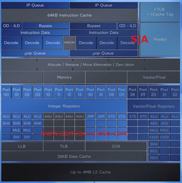
Close to informational
The block diagrams of Gracemont, and everything else, were ‘artistic renders’ or Qualcomm-level useless. SemiAccurate asked for real architectural diagrams for everything presented, after all this was architecture day, and the Gracemont folk were the only ones that provided the above diagram which is miles ahead of the presented ‘artistic renders’ but nothing close to what we need. See the Tremont link for why. That said, baby steps, what did we expect at a day labeled architecture?
Gracemont appears to be a mild tarting up of Tremont with added AVX-256 but not -512 or AMX, VNNI, and possibly more but who can tell? The net result is a claimed 40% performance uplift at ISO power or 40% power savings at ISO performance. Vs Skylake. Really? With one thread on SKL. For a 2C/4T SKL vs a 4C Gracemont the numbers go from 40% to 80% but all the fine print was linked to pages that were not live so we can’t tell you how they scammed the numbers.
That said they are implementations not ISO process so the overwhelming majority of those gains are process based. In that light Gracemont is nowhere near as good as they want you to think. And they want us to write. They also directly avoided comparing the cores to the previous generation for some reason, any guesses how it would fare vs a Tiger Lake core on 10++? The big cores were compared to 11th gen for some reason so it looks like they had access to those parts to test. When we asked for those numbers we got denied on ‘product’ grounds. How are we supposed to evaluate an architecture if you don’t give us basic comparison points. Based on what they gave, Gracemont has a lot to hide. About the only good thing we can say at this point is that Intel claims you can put four of them in the footprint of a Golden Cove but that seems to be a GC without AVX-512.
Golden Cove:
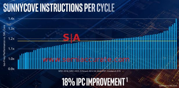
Speaking of big cores we come to Golden Cove, the newest Intel core based on 10+++… err… SuperFin+… err… 7 but not 7nm. It bumps up allocation from 5 to 6 wide, adds two execution ports for a total of 12, and is ‘smarter’. How? Beats the hell out of us. Everything else is a little more here and there, a few instructions optimized, and a few little additions here and there. It all adds up to a claimed 19% performance improvement at ISO frequency, that is a killer improvement right?
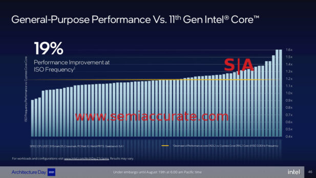
19% performance uplift is vs 11th Gen is great!
If you read the fine print, it compares against an 11th gen Intel Core CPU, so Tiger or possibly Ice, right? That 19% is pretty solid for modern processors on a similar, 10+++ vs 10++, process so Intel did good here. Unfortunately they took the low road and compared it to a 14nm Rocket Lake CPU. Why? Think about it or look at the slide below. It will probably be justified on the grounds of desktop vs desktop while conveniently ignoring the fact that this is a core to core comparison and Alder has mobile parts in the same power envelope. Tight embargo lifts are good at making people miss things like this.
This chart may be problematic for marketing
The Ice Lake core has an 18% improvement vs Skylake core, Rocket is slightly up on Sky so it looks like Golden Cove is a whopping 1-2% better than Ice/Tiger Lake cores. Be still my beating heart. Intel was asked but would not provide the same comparisons vs a 10nm core citing product vs architecture, something that wasn’t a problem when comparing to 14nm cores. Strange that.
AMX:
AMX looks really interesting, albeit for a limited set of use cases like AI. It uses Tiles, basically a set of eight 1K registers that are filled with matrix data and fired off in a co-processor fashion to a Tiles unit/pipeline/coprocessor. There were vague hints that this architecture could be used with a coprocessor or something else but it is unclear and there wasn’t time to get clarity. We also wanted to know what instructions the AMX unit had, just 8-bit multiply/TMUL or other data types and operations? Again no answers. AMX could be a good thing or it could be BS that no one wants, we have no way to tell at the moment.
Thread Director:
Thread Director is a new hardware unit that takes performance measurements on a much more granular level than previous counters and gives hints to the OS. This ostensibly enables Intel to do Big/Little on Windows just like ARM but theirs is better because they say so. Tech was vague here, lots of ‘go us’ and lifestyle choice fluff but almost no actual tech. That said we managed to peel a little out of Intel in time but first an aside.
Intel’s position on heterogeneous cores is that if you need to do a big and little core in one system, you don’t know how to design cores. Really, they told us this directly multiple times. That means Thread Director and Alder Lake are proof that Intel’s woes of late are not process related, they are due to incompetent architects. Before said architects write angry emails to me, let me point out that your beef is with the PMs and similar people who repeated this message for years, not with us for repeating it. That said feel free to send us a long letter telling us how ARM was correct all along and pioneered this awesome tech, we would be happy to publish it.
Back to the point, what does TD do? It looks at load on a CPU and gives feedback to the OS as to what threads should go on what cores, big or little. After far too much pain, we got that it bases decisions on busy-spin detection for operations usually used in graphics, thread pools and contended locks, instruction mix, efficiency of execution in terms of IPC, bottleneck classification in terms load/store latency and execution. Basically overview level obviousness, not architecture but we will take the scraps we can get for now.
All this said TD is a waste of time and silicon. Why? Big/Little on a phone makes a lot of sense, it is always on, has a tiny battery, and needs to save every milliwatt it can. A PC has a big battery and can sleep cores for the majority of time between keystrokes, the potential savings from a small core aren’t even rounding error, they are likely dwarfed by things like keyboard backlight draw. The downsides of putting this level of complexity on a broken paradigm like Windows is painful to contemplate, Microsoft may be on board officially but they are likely just handing Intel the work Qualcomm did and you know how well WARTbooks work.
TD is ONLY compatible with Windows 11, Windows 10 does not have the tools to see TD data much less use it. Intel went to great lengths and had painfully tortured logic to say that Windows 10 has a lot of heterogeneous core capabilities without TD. It doesn’t. Heterogeneous cores on Windows serve one purpose, so Intel can catch up with AMD on the core count marketing slides. The fact that it is a painful and broken paradigm requiring currently non-existent software support means users are going to suffer for this marketing game. On it’s own, TD does absolutely nothing in a closed loop fashion, it is wasted silicon and power for the majority of customers.
There is absolutely no reason for Intel to go big/little and lots of reasons for them not to, it is just dumb. For the record when asked, Intel said they would not comment on Linux support because, wait for it, that is a product decision that may be disclosed closer to launch. So like the 10/14nm comparisons above, things that can be spun as good are architecture, things that are not as good are product decisions. Got it. I just wish Intel would be honest for once.
Alder Lake:
Alder Lake is one of the most anticipated Intel CPUs in a long time, mainly because they are finally breaking down and copying ARM’s Big/Little. It is more like anticipating a car crash than waiting for a game changing tech but we will take what amusement we can get. AMD has been delivering real 16C desktop CPUs for years now, soon Intel will be able to claim the same number, albeit fake, of cores. Yay marketing.
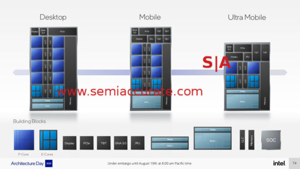
Talk about architectural details…
Yay, Intel put up block diagrams? Oh they are artistic renders that don’t actually convey what is really going on and contradict the version on the next slide? That architecture is not an architectural issue, right? In any case there are three Alder Lakes, big/little, bigger/little, and biggest/little with two, six, and eight big cores plus eight little cores, marketing seems to rule here. In any case TBT stands for Thunderbolt, GNA is Gaussian Neural Accelerator, and IPU is image processing unit.
That leads to a few interesting observations, the desktop Alder does not have an IPU or TBT block. I guess Intel’s insistence that their IPU were not useless on a non-mobile platform has now changed in light of something new in this generation. Not sure what that could be, lots of people take pictures on their phone and process the raw data on their PC, right? There has got to be a portion of a benchmark somewhere that uses the IPU, anyone know what it is?
On the Thunderbolt side, this proprietary feature uses a lot of silicon area for features that literally no one uses in the real world. It is on a lot of machines because MDF and slush funds make it very lucrative for the OEMs to add the ports, but this should have been put to bed generations ago. In any case for some reason this amazing and useful feature is pulled out and put on an external die for desktop Alder, almost like we were right years ago.
So overall Alder put in a lot of effort to make something that will give them bullet point parity on the sales floor but is a net negative for the end user. There is no excuse for Intel to not use that die space for two more larger cores, period. Could it get worse? Sure.
The big cores, Golden Cove, and the small cores, Gracemont, finally have ISA parity. They got there by adding AVX-256 to the small cores bloating area significantly, and removing absolutely key features that users need from the big cores. That last bit was Intel’s line, not ours, we have been saying those features, specifically AVX-512, are idiotic on consumer cores for a long time. This time around things like AVX-512 and AMX are either not present on the large dies or fused off. Those indispensable user necessary features could possibly be a little less necessary than was implied for the last decade because this time is different or something.
Intel has many artistic renderings that are all accurate
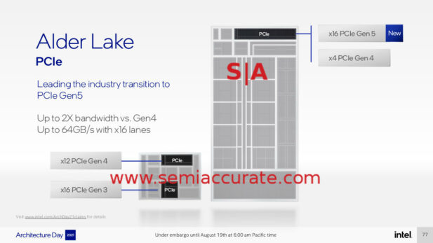
Then there is this slide on PCIe. Gen5 was touted as the killer app of Alder Lake even though there are no cards that use it. That said the slide above seems to intone two things. First the artist rendering of architecture in the previous slide was not all that accurate and most Alder dies don’t appear to have PCIe5. We specifically asked about this and it wasn’t even denied with a, “that’s a product thing” blow off, it just wasn’t answered. The questions before and after it were, take this as you wish.
The Rest:
That brings us to the last six topics, XeSS, XeHPG, Xe-Core, Sapphire Rapids, XeHPC/Ponte Vecchio, and Mount Evans. There is likely a lot of amazing architectural detail in these products that Intel didn’t talk about, after all this was Architecture Day. Some of these we managed to peel out of Intel and would love to share but at this point we have no more FSCKs to give. Until Intel decides to do radically different things like talk about architecture at Architecture day and give us enough time to get questions answered before we have to write, said FSCKs will not be given, I have wasted far to much of my life trying to work around intentionally bad scheduling decisions. Enough with the half-truths, comparisons skewed well past the breaking point, and more. If I hear “That’s a product decision” once more on basic architecture questions….S|A
Charlie Demerjian
Latest posts by Charlie Demerjian (see all)
- Intel Bumps Xeon Memory Speeds - Jul 20, 2026
- Qualcomm’s 2026 Investor Day Has Hidden Goodies - Jul 15, 2026
- Phison Phudges The Numbers… In A Good Way - Jun 24, 2026
- Who Are The Qualcomm Enterprise Customers? - Jun 23, 2026
- Innodisk Adds 10GbE To Useless M.2 Slots - Jun 19, 2026