 One of the most interesting technologies shown in 2018 was Intel’s Foveros chip stacking. It may not have been the holy grail of semiconductors but it ranks as at least an anointed stein.
Lets be clear about this, Foveros is something between a very advanced iteration of what was and a big step toward the end goal of arbitrary chip stacking but it doesn’t quite make it all the way. That said it is a very cool thing that will have some very interesting applications beyond what was shown off at Intel’s Architecture Day. To explain what Foveros is and what it isn’t, lets look at the details.
The demo of Foveros
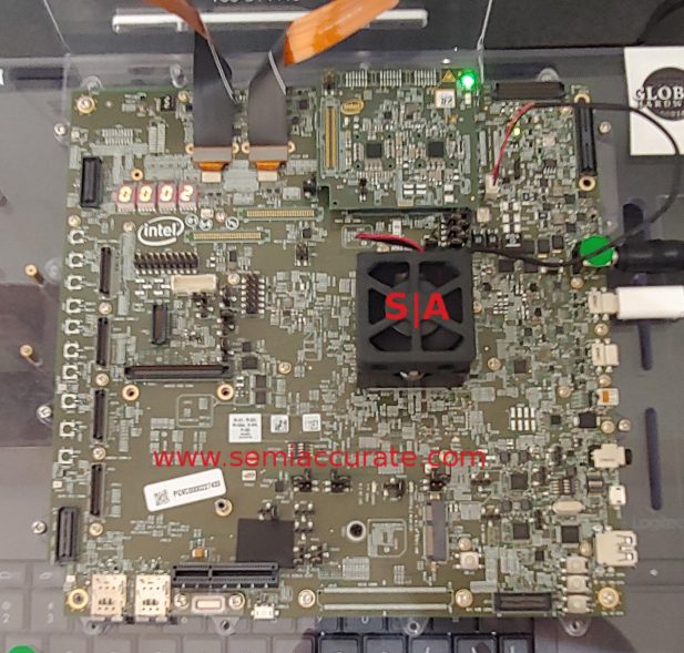
What you see above is the first public showing of Lakefield, the first product based on Foveros technology. It is a big.Little system with four ‘small’ Atom cores and one ‘big’ mainstream Ice Lake-ish core. Intel said it was designed for a specific customer and comes in a 12x12mm package. For those of you not up on packaging minutia, that is the standard dimensions for cell phone/tablet SoCs. (Note: Feel free to insert your own joke about Intel’s commentary on ARM’s big.Little and how they would never need to do it themselves, it is too easy for us professionals. We would get no points because the complexity multiplier is zero.)
Foveros with Active Interposers
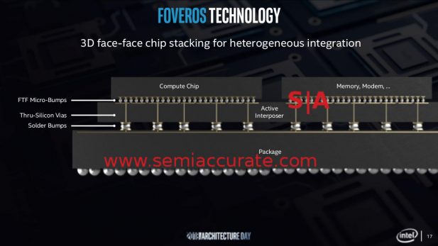
The first diagram of Foveros that Intel showed off was a CPU and radio mounted on an active interposer. This is pretty standard stuff, nothing new here or at least nothing new revealed yet but we would be surprised if there were not hidden twists yet to come. Why aren’t we excited? Because IBM showed off a much bigger and hotter die version almost seven years ago at Common Platform 2012. AMD, Xilinx, and dozens of others have been shipping products on passive interposers too, it is old hat by now. So what is new? Take a look at the diagram below.
Foveros die on die
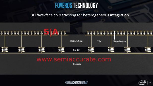
The first diagram was just an active interposer but this one has two active dies mounted face to face. Unless you count the hundreds of millions of cell phones out there, this one is unique. Actually we would consider Foveros to be unique in this situation for one reason, power. Unlike cell phone chip stacks which avoid the biggest problem of chip stacking, heat, Foveros doesn’t. Sort of.
Heat is the problem with stacking and the aforementioned holy grail is to arbitrarily stack hot dies on hot dies without the problems of bump cracking, things melting, and power distribution headaches. Cell phones which run in the low single digit watt range avoid this by not using enough power for it to be a big problem. With hot/hot dies you need to pull that heat out from the bottom layer and silicon is a great insulator so up is not a great way to do it. At the moment since there have been no real hot/hot die stacks shown by anyone, it looks like the solutions aren’t obvious or near term.
Coming back to Foveros we have the middle ground which is why we called it an anointed stein, it is a hot die on top of a cool die. This is something SemiAccurate has not seen anyone else publicly demonstrate before, it is pretty unique. You can look at this as avoiding the problem or doing some clever engineering to get us part of the way there, SemiAccurate thinks it is the latter. Intel obviously avoids the heat generation on the lower die by putting the Atom cores there, but the top die is still hot and there are a lot of problems that even that brings.
The biggest of these problems is power distribution, hot dies obviously consume more energy to do their job so how do you get it to the top die? The obvious answers take a huge amount of die area so novel approaches are needed. That said, Lakefield is a product and will presumably be shipping so you can assume Intel solved these problems.
Lakefield Foveros
If you look at the Lakefield diagram you can read a few interesting things into it. One is that Foveros is a 2-high stack, face to face, technology not a multi-die stack ala HBM memory which currently goes to 8-high with TSVs instead of face to face. With the caveat of, “this is just an illustrative diagram, not a technical one” you can also see that the memory is connected to the package, not the top chip as one would expect. This means you don’t have to put lots of TSVs through your high value 10nm die sucking up lots of area. In this sense Foveros is a lot more conventional construction.
Foveros on an FPGA
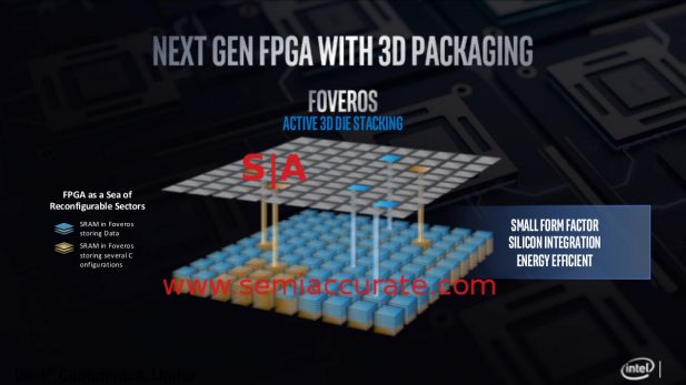
The most interesting thing about the technology is the flexibility it allows. This goes beyond the usual mix and match process tech that conventional packaging technologies and chiplets like AMD’s Rome allows for. Foveros will allow things like putting blocks of functionality, be that memory, I/O, or whatever, close to the parts of the chip that consume or produce data for it. The trick with Foveros is that those blocks can be in the Z dimension, not X/Y, and can be on a different die, process, and power rail. As you can see above, Altera sees this as putting memory and storage closer to the blocks that use it. From that simple concept you can run wild once stacking comes in to play for real.
So Foveros is the real deal but not the end goal. It is the first big step toward the goal of arbitrary hot/hot die stacking we have seen in years, the last one being IBM’s active interposer shown in the early part of this decade. Until the next big step, Foveros looks like it will give Intel some real advantages in both packaging and flexibility but as always the devil, and the capabilities, are in the as yet undisclosed details.
That said SemiAccurate can shed a bit of light on two questions, who is it for and how Intel is solving the power distribution headaches.
Note: The following is for professional and student level subscribers.
Disclosures: Charlie Demerjian and Stone Arch Networking Services, Inc. have no consulting relationships, investment relationships, or hold any investment positions with any of the companies mentioned in this report.
Charlie Demerjian
Latest posts by Charlie Demerjian (see all)
- Nuvia Founders Have A New Startup, Nuvacore - Apr 16, 2026
- Nvidia Is Negotiating To Buy A Large PC Oriented Company - Apr 13, 2026
- Dell Does Modular Laptop Boards Right - Apr 7, 2026
- Qualcomm Snapdragon X2 Review Embargo Lifts Tomorrow Morning - Apr 6, 2026
- Intel Cuts HDR OLED Panel Power with SmartHDR - Apr 2, 2026


