 Calxeda just launched what is quite possibly the most important new chip this year, it will change the game. On a curious dichotomy though, we don’t expect this version to set the market on fire, but the architecture will definitely change how things are done.
If you have been reading SemiAccurate for a while, you know we are following the whole yet unnamed space that Calxeda is aiming for quite closely. To describe it simply, it is a box with a lot of small CPU cores packed in with densities that are, well, fast approaching silly. SeaMicro is the current pacesetter here, they have a 10U box with 768 Atom cores packed in to it. If you read that in a Rick Moranis voice, you get the idea.
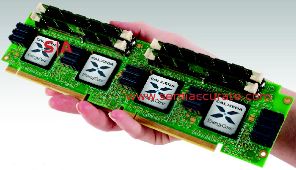
Four sockets, 16 cores, 20W, one hand
That brings us back to Calxeda, and their new chips called the EnergyCore ECX-1000 line. As you can see, the board itself is not that big, and supports four chips, SoCs, or whatever you want to call them. While SoC is closest, the EnergyCore line has the system fabric on board, so it is in some ways more than a SoC, but once again, hard line definitions are not all that apropos here.
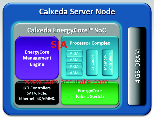
Each chip has 4 ARM A9 cores running between 1.1 and 1.4 GHz with full NEON 128-bit registers. It is a vanilla ARM core, not an architectural reworking ala Qualcomm, development effort was spent in places with a much higher bang for the buck. Those cores are backed by 4MB of L2 cache and a memory controller that supports ECC and low voltage DDR3 at 800, 1066, and 1333MHz. Since the A9 core is 32-bit, the memory is limited to 4GB/socket, something that will limit the addressable workloads until an A15 based part is released. All of this is the block labeled core complex.
Many blocks for many cores
Next up is the box labeled I/O controllers, and it is just what it sounds like. You have the obvious housekeeping port for booting and control, plus an SD/eMMC controller. For heavier traffic, you have four PCIe 2.0 controllers that allow up to 16 lanes in total, and five SATA 3Gbps ports in case you have an aversion to network booting. Overall, so far, so fairly common.
With that in mind, the other two boxes are where the magic, and likely most of the effort, went. Calxeda likely spent most of their effort on the Management Engine and Fabric Switch boxes. These two chunks are what set the ECX-1000 SoC apart from the average ARM chip, and move it from the tablet space to the server arena.
The management engine is a Baseboard Management Controller (BMC), basically a little chip that lets you tweak the server to your hearts content remotely. A good BMC makes all the difference between a manageable server and something that sits in a remote data center consuming power and generating errors at a high rate of speed.
With a good BMC, you can control your server, boot, bare metal install, manage, and twiddle with all the settings you want, all from any PC that can reach the box across the internet. These used to be a pricey option on high end machines, but lately, they are becoming low cost or free options. Intel deserves a lot of credit for pushing this idea with vPro, but you can go way up from there. Changes to how servers are hosted, clouds, virtualization, and security have all made a BMC pretty much mandatory in a modern server.
Calxeda decided to put a BMC not in each server, they put one in each chip/node. This may sound like a waste of resources, but remember, we are talking about a big box of shared nothing chips, not a fully coherent monster. If you are leasing servers to customers, you can give them their own machine, their own management controller, and let them screw things up on their own, or you can manage them all yourself. The key take home message is that there are options for the system designer and admins.
That flexibility is nice, but the programmability of the last box, Fabric Switch, is probably the single killer feature of the ECX-1000 chips. There are eight 10Gbps links to that switch, three internal, five external, use as many as your architecture needs. Each channel can be configured to run at between 1 and 10Gbps, and will dynamically scale based on load and power configurations. If you care more about deterministic latencies, you can lock them at a given speed, but most people will probably trade the mild latency gains for the power savings. Calxeda claims about 200ns latency between directly connected nodes.
What network topology does a Calxeda server use? That is the killer feature of the Fabric Switch, the network topology is completely configurable. If you want to put five links between two chips, you can. Small scale direct connect? Redundant connections? Thin or fat trees? Rings? All are not a problem. The links are seen by software as vanilla ethernet, no drivers needed, and everything is completely transparent to the CPUs. Each chip has two MACs, so the software side should be about as simple as you can ask for.
When a server is designed, the topology is obviously fixed, wires don’t tend to auto-configure well. The Fabric Switch does not do any autodiscovery, you need to pick a topology at design time, but what that looks like is up to you and your needs. From there, you run a Calxeda supplied tool that builds a routing table, and that is burned on to the SoC’s flash. Initial designs are said to be moderately fat trees, but you can expect more exotic architectures as more customers kick the tires.
Why is this a killer app? Most servers are set up to be generic, either fully coherent or shared nothing. Coherency has a high cost, shared nothing is relatively easy but usually pays a price in latency between nodes. If you have a workload that would benefit from a more specific type of network, you can design your own chipsets and interconnects, but the cost is prohibitive for all but the largest customers.
With the Fabric Switch built in to each core, building a custom network is not a theoretical possibility, it becomes almost practical. If your workload is amenable to a solution like the EnergyCore chips, the network won’t be an impediment or a bank-breaker. This is a killer feature for the space that Calxeda is aiming their chips at, and it’s importance is hard to understate.
The marketing pitch from Calxeda is performance per watt, and here too, they seem to have delivered. Officially, the entire SoC and a DDR3 DIMM suck 5W at 100% CPU load and will idle a <.5W. A four node card like that pictured above pulls a mere 20W, and we really think Calxeda hit that mark. Why? Look at the HP system below, specifically the power distribution board in the center between the two watermarks.
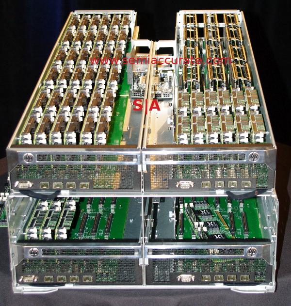
HP Calxeda server, or is it 288 servers?
This is the 4U, 4 tray HP rack mount box, an SL6500 chassis to be exact. Each tray is 2U x .5U, so 1U in volume, and contains up to 18 Calxeda EnergyCards, each one is a four node reference design. That would mean 72 nodes/servers per U, 288 cores. A 4U box would contain 288 nodes and 1152 cores. Back to the power side, each tray has a small power distribution board in the center, and it is fed by two 6-pin PCIe Graphics connectors (PEG), and has mounting brackets for one more board.
Update: 11/3/11 The HP chassis is an SL6500, not an SL65 as originally stated.
Each PEG can supply 75W total, so that means a tray has a max supply of 300W, 16.67W/board, 4.17W/node average. This is a prototype box, and HP doesn’t have to stick to the PEG limits, it may only be using the physical connector, but it shows that Calxeda is definitely in the ballpark of 5W/node for their initial samples.
If 5W/node is more power than you are willing to spend, or your task is severely bound by something other than raw compute power, Calxeda has parts as low as 1.8W for a 2 core CPU with less cache. Whatever you choose, the sheer performance per watt is hard to beat, impossible in something that scales up to the same 4096 node count that the ECX-1000 hits.
All this tech is wrapped in to a single <5W chip made on a 40nm process at TSMC. They are sampling soon and should be widely available in the middle of 2012. As you might have heard, HP is the big OEM making servers based on Calxeda chips, but there are others.
At the launch event Tuesday, there were some interesting names on stage, and more interesting names off of it. Only one customer was officially mentioned, the financial firm Cantor Fitzgerald, but some names I noticed in the crowd were Zoho, VMWare, lots of financial companies, and many more that asked not to be mentioned. Although the author didn’t attend, HP told a friend at their event earlier on Tuesday that they were working with, “the top three social networks” using this design. Who would have guessed?
That is the tech behind the chip, the box it fits in, and the wires that run all over the insides. Having a 288 socket/U design with well over 1000 cores/U is all fine and dandy, but what on earth would you use it for? Why would anyone want to own one, much less pay money for it? What was I smoking when I said the Calxeda EnergyCore ECX-1000 would change how things are done? Those are mighty good questions, stay tuned.S|A
Charlie Demerjian
Latest posts by Charlie Demerjian (see all)
- Nuvia Founders Have A New Startup, Nuvacore - Apr 16, 2026
- Nvidia Is Negotiating To Buy A Large PC Oriented Company - Apr 13, 2026
- Dell Does Modular Laptop Boards Right - Apr 7, 2026
- Qualcomm Snapdragon X2 Review Embargo Lifts Tomorrow Morning - Apr 6, 2026
- Intel Cuts HDR OLED Panel Power with SmartHDR - Apr 2, 2026


