 SemiAccurate told you all the details about AMDs Jaguar core in Kabini last August, now the company is talking about the rest of the SoC too. Lets take a look at what the Kabini uncore does and how it goes about doing it.
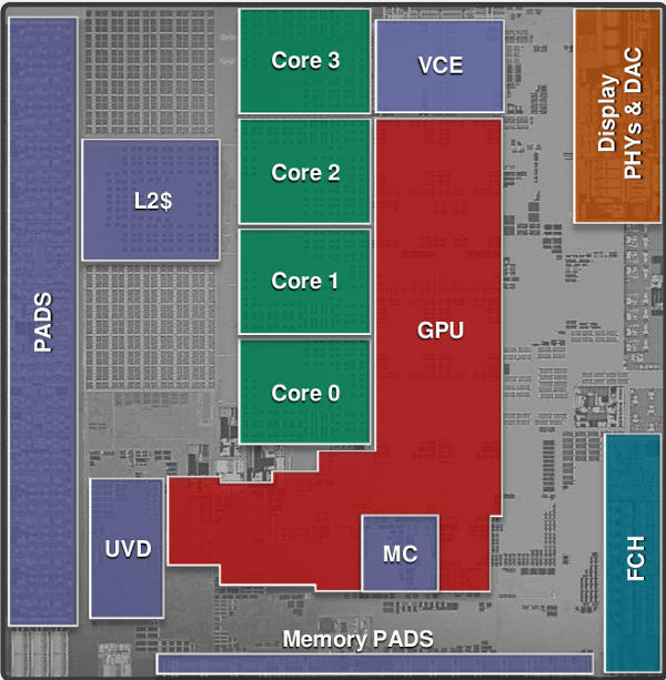
If you recall Kabini is the smaller AMD SoC, the successor to Brazos and it’s Bobcat core. The Jaguar core is of course all new and the rest of the SoC is almost all new too with very little carried over from previous parts other than the shaders and some generalized architecture paradigms. Take 2-4 Jaguar cores, 128 Sea Islands (HD8000 class, the real HD8000 not the fake renames), and the full chipset and you end up with Kabini or Temash depending on the intended market. They are the same silicon so for this discussion they are interchangeable. It all looks like this.
Die plot labeled for your convenience
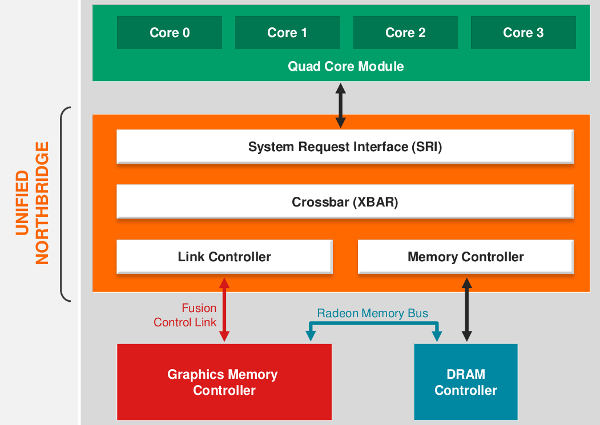
So what is new? The biggest thing is that Kabini is a real SoC in every sense, there is no chipset any more it is all one die. This is a huge win for phones and tablets, not that Kabini or Temash is aimed at phones mainly because TDPs of 3.9-25W precludes that market. That said, for higher end tablets it is a monstrously powerful device for the wattage used, especially on the GPU side. The most interesting part of the new SoC is the Unified North Bridge (UNB), basically what used to be called the chipset. Lets look at what this pretty complex piece of the puzzle brings to the table.
UNB is the nervous system of Fusion architecture
Conceptually the UNB is a refinement on the one found in Trinity, the last big core fusion part. This is a good thing, no make that a really good thing. The UNB has three main parts you should be aware of, the System Request Interface/Queue (SRI/SRQ), the Fusion Control Link (FCL), and the Graphics Memory Bus (GMB). There is also an important bit called the Radeon Memory Bus (RMB) as well as the associated parts of the blocks connected by these links. These do nothing less than take spaghetti and turn it in to what appears to be a seamless whole to the end-user.
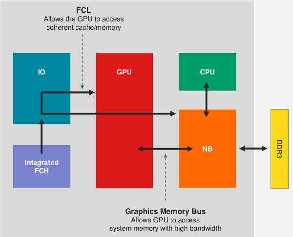
GPU busses aplenty, all for good cause
The whole point of the Fusion architecture is to have a single flat memory space that both the GPU and CPU can see and access at the same time. This allows a coder to do all sorts of neat tricks while the CPU saves time and power by not having to copy data back and forth between units. The FCL and RMB were introduced in AMD’s LLano with the code names Onion and Garlic, then massively beefed up for Trinity. Llano’s Pin-in-Place and Zero Copy evolved into much broader visibility of CPU and GPU memory in Trinity, and at least in the guise of the PS4 that wall has been erased nearly totally. The PC is still hobbled by Microsoft’s inability to code their way out of a paper bag though, so it probably won’t be fully exposed in PC form. That is a true pity.
The reasoning behind this architecture is simple enough, GPUs usually need data once and rarely write back to memory while CPUs tend to reuse information and write quite a bit. GPUs therefore need far less cache than a CPU and will quickly pollute any cache shared with the CPU. All of this has to pass through a single DRAM controller to keep all the units from stepping on each other’s toes. How do you route the correct information to the correct functional unit? That is where the FCL, RMB and GMB come in, they allow a single memory controller to orchestrate other units to act directly and correctly.
Once something comes in to the DRAM controller, if it is meant for the CPU it goes across the GMB, essentially what normally happens in a CPU. In this case the bus is 256b wide, more than enough to support everything the chip needs to pass around internally. This is more or less analogous to the old FSB but is a lot faster and smarter.
The UNB also connects to the GPU through the FCL, the direct shortcut between the CPU and GPU. This is where much of the magic happens, if the CPU needs to pass something to the GPU directly, or the other way around, it goes across the FCL. This is a 128b wide path that gives the CPU direct access to the GPU frame buffer, something that wasn’t previously possible on a PC without a lot of pain and hoop jumping. It will also allow you to do all sorts of graphics tricks like complex texture and graphics manipulations in real-time with very low overhead.
In a move that initially sounds a bit strange, the FCL uses a command structure that is very similar to PCIe to pass data between the UNB and the GPU. Using PCIe is actually a genius level move on AMDs part because it effectively means all the old code, drivers, and communications minutia will see the FCL as a PCIe link. More importantly is that the SRQ, the block that controls what goes where, how, and when, can reroute traffic almost on a whim. If you want to have seamless switching between integrated and external GPUs, this makes life easy. Direct CPU access to the frame buffer also removes the biggest headache here too.
The last bit to look at is the RMB, the link between the GPU and the DRAM controller. What this does is effectively shortcut the path between GPU and memory vastly lowering latency. The intelligence behind every device’s memory usage is still in the main memory controller located in the UNB, but once it tells the GPU memory controller to do something with memory, the GPU memory controller can just do it via a direct path. This saves a lot of chatter between units and several needless hops for any data going to or from the GPU.
In concept, the whole process makes complete sense, everything is done via the most direct path available. There are links between all of the major units in the SoC and all transactions that don’t need to happen are simply not done. Simple as this sounds, keeping this all in sync and not having one unit step on the other is an extremely complex and painful process. If you just think about the timings involved with the memory controller in the UNB signaling the GPU to save something to memory, then making sure that nothing else touches that memory in the mean time, the complexity is kind of mind-bending. Add in radically different clock speeds, bus widths, and caching needs and you have a verification nightmare. That said, Kabini is the third generation Fusion architecture on the market and it does actually work. It isn’t simple under the lid though, not by a long shot.
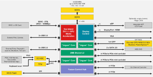
The Kabini SoC family tree
The CPU and GPU are the major internal components, but what about external devices? As you can see in the diagram above, Kabini is a true SoC in the sense that you can make a system with little or no other logic or controllers. It has eight USB2 ports, two USB3, and supports two 2560*1600 DP1.2 monitors simultaneously. It will also directly interface with DVI, HDMI, VGA, and eDP but the two monitor limit remains. There is a 4x PCIe lane for MXM cards along with four 1x lanes for whatever you want. On the memory side there is one 64-bit bus supporting two SoDIMMs at 1.5, 1.35, and 1.25v up to 1600MHz. Current sockets support up to 32GB per system, more than enough for this class of SoC.
Last but far from least is the GPU side of Kabini. Both Temash and Kabini have 128 Sea Islands shaders on all SKUs, quite the refreshing change from the old variable counts. These are DX11.1, OpenGL 4.3, and OpenGL ES 3.0 capable units that leave nothing on the table as far as specs go. This is the first time AMD has put a bleeding edge GPU in an SoC, lets hope this is a trend that they keep up from this point on. With low latency, complete CPU access to all GPU memory, and nothing left out, a talented coder could do some pretty amazing things with the GPU in Kabini. Look for this to shine in both the PS4 and to a lesser extent, the XBox One.
All in all the Kabini and Temash chips are conceptually nothing new, just refinements on a good system in every way. Power use is dropped fairly radically, performance is way up, and all the features that Llano, Trinity, and Brazos teased us with have finally arrived. Unfortunately due to Microsoft, PC users won’t get to see many of the cool features but they will be there in the PS4 at the very least. By the time the next version ships, with a little luck end users will have access to the full Fusion potential. Until then Kabini brings us tantalizingly close to the goal.S|A
Charlie Demerjian
Latest posts by Charlie Demerjian (see all)
- Nuvia Founders Have A New Startup, Nuvacore - Apr 16, 2026
- Nvidia Is Negotiating To Buy A Large PC Oriented Company - Apr 13, 2026
- Dell Does Modular Laptop Boards Right - Apr 7, 2026
- Qualcomm Snapdragon X2 Review Embargo Lifts Tomorrow Morning - Apr 6, 2026
- Intel Cuts HDR OLED Panel Power with SmartHDR - Apr 2, 2026


