![]() You may not know much about Vivante’s GPUs but if you are in to tech you have definitely heard about the products that use them. Lets take a look at this little mobile GPU IP maker and their products in great detail starting with the non-technical to get you up to speed and then dive deep in to the technical details in subsequent parts.
You may not know much about Vivante’s GPUs but if you are in to tech you have definitely heard about the products that use them. Lets take a look at this little mobile GPU IP maker and their products in great detail starting with the non-technical to get you up to speed and then dive deep in to the technical details in subsequent parts.
Vivante Corporation is a small GPU IP house based in Silicon Valley that does one thing, makes mobile GPUs for phones, tablets, TVs, and anything else you want to put them in. They were founded in 2004, started licensing GPU IP in 2007, and taped out their first physical GPU on a TSMC 90G process in 2006. That core is 3mm^2 on TSMC’s 65LP process and passes OpenGL ES2.3 testing. While even OpenGL ES2.0 didn’t exist at the time, had it been a spec the device obviously would have passed that too. If you think back to the competition at the time, most if not all were fixed function OpenGL ES1.1 pipelines.
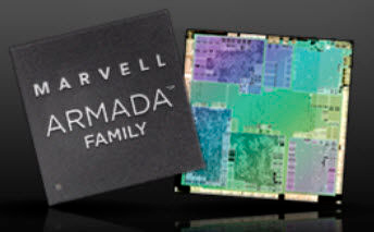
Marvell’s PXA988 SoC with the current Vivante GPU
So in 2007 Vivante cut down some features to save area and ended up with a full 32-bit precision OpenGL ES2.0 pipeline, end to end, in a footprint the company claims was the same area as other’s fixed function OpenGL ES1.1 parts. In case you are wondering why they cut the device down, every transistor adds die area and every transistor leaks even if it is not used. Mobile manufacturers, especially those on the commodity end of the market care about every tenth or hundredth of a mm^2. Convincing them that they want to take a chance on this new and upcoming spec to future proof their device is an uphill climb, not because it is the wrong thing to do but device makers are a pretty risk-averse lot.
Same for OpenCL in 2009, the old Vivante core would not do OpenCL 1.1 as is, it lacked a load/store unit. Slap one on, make a few minor shader tweaks, and voilà, that 2+ year old OpenGL ES2.0+ core is now a shiny new OpenGL ES2.0+ with OpenCL 1.1 compliance. This should tell you something about the foresight of the Vivante architects, they started a core in 2004 that would do 32-bit precision OpenGL ES2.3 and almost met the OpenCL 1.1 spec 5+ years later. But that’s not all, this first test chip from 2006 fully passed Microsoft’s WHQL testing for DirectX 9.3 with SM3.0 on Windows XP. ES2.0 didn’t exist at the time, that was a year later.
One thing to bear in mind is that DX9.3 is a superset of OpenGL ES3.0 so that 2006 test chip would probably do ES3.0 had it existed. This is an oversimplification of course, there are some inevitable minor bits to support here and there but other than cleaning up loose ends the first Vivante device was pretty forward thinking, not to mention tiny. Making a small GPU is not all that much of a trick with a modern process, making one that performs well and doesn’t guzzle power is a tough job though. How does Vivante do on these fronts? Pretty well actually.
If you look at the hardware itself, Vivante architected it for mobile usages. Most of you are rolling your eyes about now, there isn’t a GPU maker in the world that won’t tell you they architected their latest device specifically for the market in question only to turn around and tell you the exact opposite when it is shoehorned in to the complete opposite end of the spectrum. That said Vivante only makes low power, small die area GPUs for the mobile space so their claims have some credence. When you look at how they got there on a technical level, you will understand how they did it.
The first thing you will notice is that the Vivante GPUs have a pretty massive top frequency, 1GHz is the official number on TSMC’s 28LP process but more is possible if needed. On the other end of the scale the clock floor is 100MHz and the frequency is scalable in increments of 1/64th. For a 1000MHz GPU, that would be increments of a bit less than 16MHz or enough granularity for anyone’s use. The scaling is a hardware closed loop with some boundaries set-able in software. As one would expect of a modern GPU core, the Vivante parts have full DVFS capabilities along with hard power gating.
Once again making a 1GHz GPU isn’t exactly headline material of late but making q 1GHz GPU that fits in 3mm^2 on a 65nm process is a bit tougher. Especially for one that first taped out in 2006, that is quite the forward-looking architecture for you. But making a 1GHz GPU that doesn’t consume power like a Fermi? That is quite hard too, but once again Vivante did it. How can I be sure that it really works, how can you separate out the GPU power from the CPU, SoC, and device power, and how can you tell the tests aren’t rigged? Easy, go out and buy one and test it however you want. That doesn’t solve the problem of peeling out the GPU wattage but the rest should be close enough.
There are a bunch of Vivante GPUs on the market right now, maybe you are aware of Google’s Chromecast, Samsung’s Galaxy Tab 3 (7″), Huawei’s Ascend P6, or the Kindle Fire HD 8.9″? On the silicon side how about Freescale’s I.MX6, Marvell’s PXA988, or TI OMAP 4470 for starters with more undoubtedly out on the market too. You can by them right now, test them yourself, and see the results. From the informal testing SemiAccurate did with a Samsung Galaxy Tab 3 7″, there is nothing bad to report. Battery life was excellent, graphics never had a single bit of corruption or errors, and nothing crashed unexpectedly. Everything just worked. Then again if Vivante is claiming they support a version of a spec that is what you would expect to happen and they delivered.
What specs does the Vivante core architecture support? OpenGL ES1.1/2.0/3.0, DirectX 11 (9_3), OpenGL 2.1/3.0, WebGL, OpenCL 1.1/1.2FP, OpenVG 1.1, X11/EXA, DirectFB 1.4+, GDI + DirectDraw, Renderscript /FS, and EGL 1.4. On the platform side Android, ChromeOS, QNX, GHS, Wind River, Windows, and Linux are fully supported. That is a pretty comprehensive list and to make it a bit better there is a common software stack across all the Vivante product lines. Why? Because it is all one architecture, from the beginning most of the changes were removal of some features and the additions were quite minor. Once again, foresight matters.
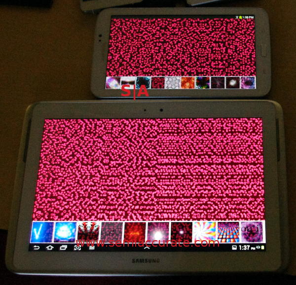
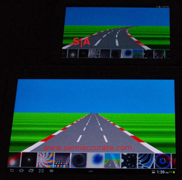
As with everything else there are specs and there are specs, all companies claim absolutely perfect support for everything but few deliver. Vivante claims their GPU is about the best you can get for graphics precision at the moment, but what did you expect them to say? Every company says this at every product introduction, and most rig tests in one way or other to show their product in a nice light. Unlike many though, Vivante is right about their accuracy claims, and the YOUi Labs shader tests show it off in pretty vivid detail.
Precision determines randomness in this test, guess which passed?
Smooth shiny balls are nice and precise, hairy balls are not
The road ahead should not be straight if your shaders are precise
As you can see the smaller tablet with a Vivante GPU on the top is able to pull off the shader tests correctly, the bottom tablet which if memory serves is an Mail-400MP4 is pretty awful. That is not to pick on the Mail-400MP4 in particular, all of the other GPUs tried failed this test, and if you look at the YOUi Labs shader precision test page, you can see why.
Update 9-6-13@3:05pm: We have been informed that the above test is against a Mail-400MP4 GPU, not an SGX544MP2 as originally indicated. It has been corrected.
Lets just say that it wasn’t a case of pass fail, more shades of painful for results. Precision pays in the details and only one GPU seems to be capable of that level of precision. That said the newest Imagination and ARM Mali GPUs were not available to test but we expect them to do much better. Before you expect perfection though realize that a full Nvidia GeForce GT630M failed the test according to YOUi. Then again all the others did too.
With all this precision, supported protocols, and everything else, how large is this beast? If you said huge you would be wrong, it is actually smaller than the competition while being more precise. Take a look at the following table that lists a competitor’s GPU, it’s die area, and the process it is made on. Next to that is the roughly equivalent Vivante GPU with the area listed normalized to the same process the competitor is on. All the Vivante GPUs listed here are 40nm part but are available on other nodes too.
Some modern mobile GPU areas with the Vivante equivalent
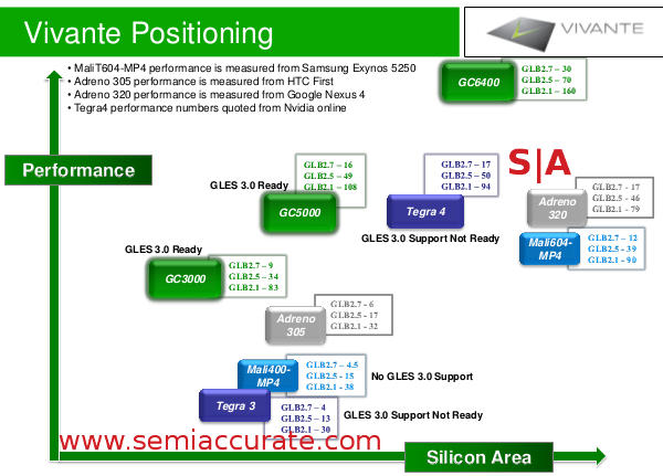
Vivante is smaller than the equivalent ARM and Imaginations competition, but how does it perform? Pretty good actually, Vivante supplied a list of benchmarks some of which were run while SemiAccurate was present some not, and Vivante’s product won the overwhelming majority of the comparisons. Not bad for a smaller GPU design that taped out in 2006, and while we didn’t directly measure the area, the few numbers that SemiAccurate could find publicly did match up nicely with those provided. Although it uses only one benchmark, GLBenchmark across three versions, the graph below gives a pretty clear view of performance per mm^2.
How Vivante sees the mobile GPU world: size vs performance
Now that you have and idea about the area and performance that leaves what is likely to be the most important metric as far as mobile devices are concerned, power use. Vivante claims they are competitive with the rest of the pack but peeling out the GPU power of an SoC is effectively impossible to do for an independent site. The only thing we can point you to is that the Vivante cores are being used in a lot of devices and none of which has any GPU related power issues. The Samsung Galaxy Tab 3 7″ SemiAccurate has been playing with has both phenomenal battery life and does not get very warm even after long gaming sessions. Anecdotally anyway the power use is quite good.
We are aware that all of the above is pretty short on hard data and long on superlatives. Normally SemiAccurate decides to dive in to the tech first then talk about the decisions, trade-offs, and fluffy stuff that accompany the hard data. Since Vivante is a relative unknown to most enthusiasts we decided to take the opposite approach to give you a feel for what you were looking at and why. Fear not, it is now time to take a deep dive in to the nuts and bolts of the Vivante GPU cores, plural for 2D, 3D, and Vector units. Stick around the good stuff starts in Part 2.S|A
Have you signed up for our newsletter yet?
Did you know that you can access all our past subscription-only articles with a simple Student Membership for 100 USD per year? If you want in-depth analysis and exclusive exclusives, we don’t make the news, we just report it so there is no guarantee when exclusives are added to the Professional level but that’s where you’ll find the deep dive analysis.
Charlie Demerjian
Latest posts by Charlie Demerjian (see all)
- Nuvia Founders Have A New Startup, Nuvacore - Apr 16, 2026
- Nvidia Is Negotiating To Buy A Large PC Oriented Company - Apr 13, 2026
- Dell Does Modular Laptop Boards Right - Apr 7, 2026
- Qualcomm Snapdragon X2 Review Embargo Lifts Tomorrow Morning - Apr 6, 2026
- Intel Cuts HDR OLED Panel Power with SmartHDR - Apr 2, 2026


