 Last week AMD let out some of the info about Fury aka the Fiji GPU, basically everything but performance. Lets take a look at what they said and add a few bits here and there.
SemiAccurate previously told you about the HBM memory that is the heart of Fiji, and in a nutshell that is the big news. The idea is simple, instead of putting a lot of high-speed power-hungry memory on the PCB, put lots of low-speed but very wide and efficient memory on a piece of silicon. That saves board space, power, assembly time, and other things but the interposer itself is fairly expensive. At the moment this unquestionably costs a bit more, net cost that is, but as volume ramps this will drop radically. We discussed a bit more about the tradeoffs here.
Other than that what is Fiji architecturally? Think Hawaii but with some more shaders and bigger caches but that’s about it. AMD hinted at some ISA differences and a few other minor changes under the hood for this Caribbean Islands architecture but refused to discuss them so, well, they can’t be that big a deal. AMD also claimed there were some major changes to the tessellation and geometry processing but again refused to go into detail. On a grand scale it all looks like this.
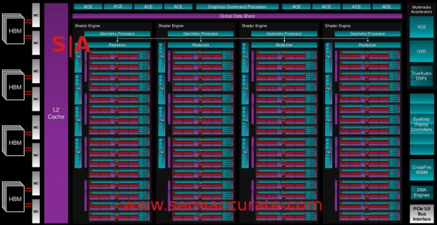
Fiji block diagram
Up top the ACE count didn’t change, it is still at eight. We strongly suspect that they are beefed up in light of the change in architecture levels to more closely reflect the HSA changes seen in Carizzo but we can’t say for sure. Like the front end, much of the back-end seems to have been carried over, with some things scaling with clock rates, others scaling with shader count as expected. The details are below, and nothing stands out as unexpected.
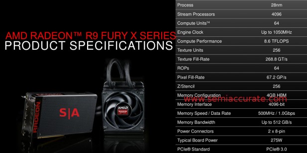
The specs for the card
Looking at the die and related silicon bits the first thing that stands out is the interposer. It is a 1011mm^2 part made on a 65nm UMC process. Since it is passive there are no transistors on it and the metal layer count is two or three, AMD would again not be specific. Since they are meant for carrying signals a long way across the die plus have balls attached, they are likely the wider, higher layer number rules, so again cheap to make. As a side note the assembly is likely done by Amkor but there are others like ASE who have the capabilities too now.
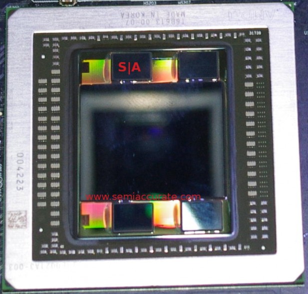
Note the colored bits by the memory
One word of warning should you buy a Fiji and molest it in various ways that overclockers and enthusiasts normally do, be careful. If you look at the above picture you can see the pretty patterns on the interposer, they look good but don’t taste good. If you want to clean off the thermal paste and replace it with your own cooling solution, be really careful of these areas. Why? Because the interposer, basically a chip, is mounted face up, it is not a traditional flip chip part with the transistors and metal layers protected by the wafer, they fragile bits are on top this time.
How fragile? Don’t touch them, don’t wipe them off, and otherwise don’t do anything that could break a far sub-micron metal trace. It is really fragile and you will destroy your very expensive GPU if you do this, don’t say we didn’t warn you. This is a tech transition that hasn’t been seen since the days when flip chips replaced wire bonding so think back to the bad old days before you mod. Really, be careful or you will end up with an expensive 4GB, water-cooled doorstop.
Back to the GPU itself the shader count goes from 2816 in Hawaii to 4096 in Fiji so the die size goes from 438mm^2 to 596mm^2, a 36% increase. AMD is claiming a 1.5x increase in performance per Watt over Hawaii, Fiji pulls 275W vs Hawaii’s 290W. You can do the math yourself but if you end up with anything other than 142% the performance of Hawaii, you did it wrong. We will have to wait few days to know for sure but assuming that number is correct, you get a very slight improvement in performance per mm^2 over the previous generation, nothing groundbreaking. Since the architectures are the same, that is about what you would expect.
Other than the added shader counts, another reason for the die size increase is greater caches. Fiji has roughly double the cache sizes of Hawaii, about 2MB vs 1MB previously, but these are distributed throughout the chip, not in one block. Basically everywhere that there was a cache, there is now about twice the cache as the old way. Look for this to help with compute tasks more than anything else, graphics should get a boost but not by massive margins.
Going back to the memory controller we have an interesting change going from GDDR5 to HBM. A lot of the GDDR5 power consumption comes from the complexity of the memory controller itself so the HBM power savings on the memory front are mirrored on the GPU itself although that number is not able to be broken out sanely. With the old way, about 25% of the die was GDDR5 controller or about 110mm^2 in Hawaii. With HBM in Fiji, it is a lot simpler even though it is wider and has a net higher bandwidth. Now only about 10% of the die is the HBM controller, roughly 60mm^2, even though bandwidth goes up significantly saving both power and obviously expensive silicon.
AMD would not comment on average memory latency and dodged the issue every time we asked. They did say that bandwidth went way way up but would not comment on latency. None of the spec sheets SemiAccurate has access to have that information but you can do a bit of back of the envelope math. The transfer rates goes from ~7Gt/s to 1Gt/s when moving from GDDR5 to HBM. HBM is simpler and wider. Prefetch goes from 8 per I/O to 2 in HBM while access granularity goes up from 32B to 256B. Given all this the first byte likely gets returned slightly slower in HBM but every subsequent byte is much faster. From there things get really complex.
That’s about all we can say about the GPU, the technical questions we had were either not able to be answered or just weren’t. Fortunately there is more to talk about that isn’t related to the die but the card itself. On the Fury X side, aka the Fiji XT ASIC, AMD finally cured their recto-cranial inversion about doing the right thing for high-end customers, and right they did. This transformation may not be of the depth of old GM vs new GM but it sure is welcome. This is the long way of saying that the new Fury X cards aren’t made of the cheapest materials and the cooling solution is not borderline painful when it ramps up.
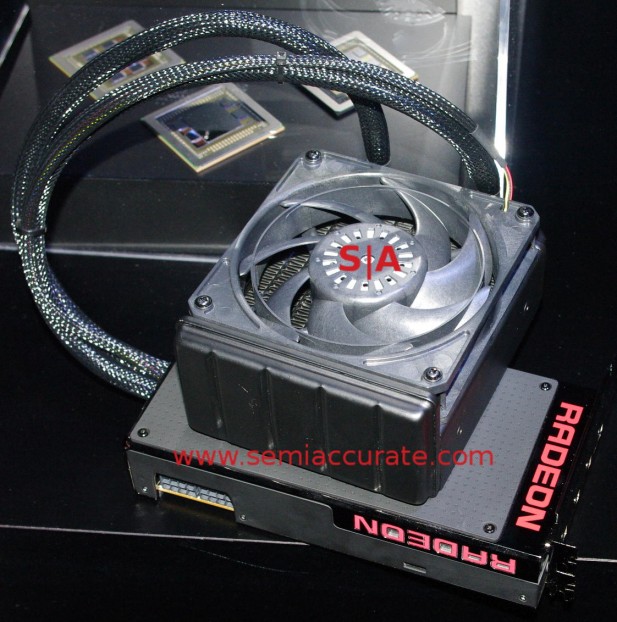
Fury X with watercooling setup
As you might have noticed the Fury X card is watercooled, and at the moment only watercooled. This is a good thing. The upcoming Fiji Pro aka Fury no X is open for AIBs to do whatever they want with so expect variants like the Powercolor UFG (Unnamed Future GPU) to come out a few weeks after the official debuts. Again this is a good thing. Last but not least is the farther afield Fury Nano GPU, basically a downclocked Fury X with a very efficient air cooler. AMD is claiming a 2x performance per watt increase on this card partially because of the 175W TDP. If you want a good example of why slower and wider works better in GPUs, there is no better data point than the Fury Nano. The lineup looks like this.
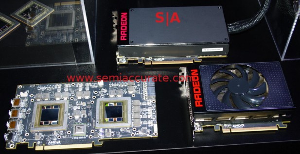
AMD Fury lineup, one, two, and less than one
Almost forgot the dual Fiji code-named once again Gemini. It is pretty but a ways out for the moment. If you do the math on the Nano, two of them would pull 350W or about what AMD dual cards of late are known to draw. Think about that for performance levels, then add a bit for cherry picked ASICs and you are likely in the right ballpark. Sizes for the cards themselves are 7.5″ for the Fury X, 6″ for the Nano, and unspecified sizes for the dual beastie.
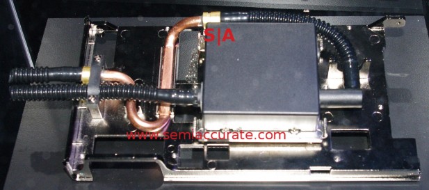
The Fury X watercooler with added finish
Back to the construction of the Fury X, specifically the water cooler. There are a few things to note here, the bulb on the radiator, the fan itself, and the flow path of the coolant. On the picture of the card itself, you may have noticed what looks like a tank beside the fan and the radiator. That is because it is a tank, there was area available in the footprint of the radiator that wasn’t taken up by the fan so AMD extended the coolant tank to hold more fluid. This added capacity allows the system to run a few degrees cooler for no added space, quite a clever touch.
Next up is the fan, even with the added tank area it fits in standard sized cooling mounts so you shouldn’t have any problems putting it in a decent case. From what we gather the water loop is made by Coolermaster so it should be a very solid and reliable piece of kit and the fan is a Nidec unit, again a good choice. On the picture of the bare cooler, you can see the intake goes directly into the GPU block then it runs over the VRMs via the copper tube. This cools the hot stuff first, then the less important bits afterwards increasing efficiency.
Those VRMs are pretty impressive too, capable of pushing out 400A if needed at 1.1-1.2V or more than enough to power the card. For the overclocking set the power circuitry is six phase and the water block is capable of shedding 500W if necessary. One looks at the aggregate numbers on the Fury X and the only conclusion you can come to is this card should have headroom.
If you look at the bottom of the cooler you can see that the metal is mirror gloss black nickel anodized aluminum, not cheap but really pretty. The panels themselves are removable via screws and are aluminum covered with rubberized material that both feels good and damps vibrations aka noise. The top panel is swappable and hopefully AMD will put the specs out there for people to print their own tops and/or make mode like cooler that fit precisely.
Additionally with the water cooler, this insulated cover on the back and front keeps the heat from adjacent devices from bleeding onto the GPU like more open designs. Even the PCB is a matte black one, something that screams attention to detail. AMD obviously put a lot of thought, effort, and care into the physical packaging for the Fury X, once again about time.
Speaking of touches there are nine LED on the PCB this time around, eight for a GPU tach and one for power. The GPU tach shows activity and can be red, blue, or both depending on which DIP switch you have on. Better yet they can be set to off if you are gaming in a dark basement room. Luckily this is not software controlled, the latency would be too high. Instead the tach function pulls data directly from the GPU GPIOs and has on board logic to light up the lights. If harnessed correctly that compute power can up the Bitcoin mining ability of the card by .0000000000000000003719%, hardly ignorable in the insane and/or OCD world of miners. The ninth LED is always green and lights up when the GPU is in ZeroCore power mode to show that it is alive.
In the end we have Fiji now called Fury, a bigger, more efficient Hawaii with a brand new type of memory. There are several minor architectural changes AMD hinted at but did not go into detail on but none of these are likely to be user facing or exposed to coders. That much is good but the construction and care taken to make the Fury X card itself is a new high for the company. AMD finally made the build quality and materials commensurate to the high-end nature of the device itself. It should be cool, quiet, and quite fast. By how much is something we can’t get into for a few more days but the hints so far are promising.S|A
Charlie Demerjian
Latest posts by Charlie Demerjian (see all)
- Nuvia Founders Have A New Startup, Nuvacore - Apr 16, 2026
- Nvidia Is Negotiating To Buy A Large PC Oriented Company - Apr 13, 2026
- Dell Does Modular Laptop Boards Right - Apr 7, 2026
- Qualcomm Snapdragon X2 Review Embargo Lifts Tomorrow Morning - Apr 6, 2026
- Intel Cuts HDR OLED Panel Power with SmartHDR - Apr 2, 2026