![]() Everspin is now sampling really high density 256Mb MRAMs with 1Gb to follow soon. When SemiAccurate told you to look out for their partnership with Globalfoundries, we weren’t joking.
Everspin is now sampling really high density 256Mb MRAMs with 1Gb to follow soon. When SemiAccurate told you to look out for their partnership with Globalfoundries, we weren’t joking.
Lets start this off by saying that we were wrong about densities, we earlier guesstimated that the first GF products would be in the 64Mb range. Instead they start out at 256Mb, sampling now, and will have 1Gb versions coming later this year. If you look back to when SemiAccurate was first talking about Everspin products in 2013 they were shipping a 1Mb MRAM.
Update April 14, 2016 at 10;55am: 64Gb -> 64Mb,
In about 3.5 years they have increased density by 16x or four doubling, not a bad progression.

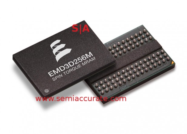
The new MRAMs look like chips don’t they?
There are some interesting details hiding in the press release though, particularly about MRAM types. The currently sampling MRAMs are 256Mb in-plane magnetic tunnel junction (MTJ) products but the upcoming 1Gb versions will be perpendicular MTJ (pMTJ) products. The interesting bit is that Everspin says that the shipping 256Gb versions will also be pMTJ based. Why is this important? Density.
While we don’t have any specific evidence to back this up for MRAMs specifically, perpendicular structures tend to take up less wafer area than planar ones. You could assume that the in-plane MTJs cells will be a lot larger than the pMTJ ones so the shipping 256Mb pMTJ devices will be a lot smaller than the sampling ones. Since Everspin is sampling the 256Mb devices to clients that are in the embedded and high availability spaces, this strongly intones that the performance of the two cells will be equivalent.
That brings us to another aspect of processes, the node these devices are built on. Everspin initially said that the GF partnership would initially be on the 40nm and 28nm nodes, but no specific process was mentioned in today’s release. Is the 256Mb product on 40nm and the 1Gb on 28, or is 28nm reserved for the promised future density increases. Either way these products represent a huge leap in NVRAM density.
Update April 13, 2016 at 3:31pm: Everspin just confirmed that the 256Mb die is on the 40nm process, the 1Gb is a 28nm chip.
Another interesting technical tidbit is the interface, until now Everspin’s MRAMs used a standard DDR3 interface, something the 256Mb product continues on with. The upcoming 1Gb products will move to a DDR4 bus so you can tell where it is aimed. Both versions are true NVRAM so you can instantly power it off, there is no wear leveling needed, and write speeds are a claimed 10,000x faster than NAND flash. To operate on the DDR3/4 busses you would need that level of speed so this number seems quite reasonable.
So in the end the news is of course that Everspin just jumped way ahead of the density curve that SemiAccurate was expecting. They may not have hit the same density as modern DRAMs but they are now working in the same order of magnitude rather than 2-3 off, a massive gain which opens up a whole new set of markets for ST-MRAM. This is going to get really interesting when products start shipping, it allows for a whole new set of devices that could not be done before. Neato.S|A
Charlie Demerjian
Latest posts by Charlie Demerjian (see all)
- Nuvia Founders Have A New Startup, Nuvacore - Apr 16, 2026
- Nvidia Is Negotiating To Buy A Large PC Oriented Company - Apr 13, 2026
- Dell Does Modular Laptop Boards Right - Apr 7, 2026
- Qualcomm Snapdragon X2 Review Embargo Lifts Tomorrow Morning - Apr 6, 2026
- Intel Cuts HDR OLED Panel Power with SmartHDR - Apr 2, 2026