 One of the most interesting aspects of AMD’s Epyc architecture is the interconnect network. SemiAccurate has talked about it in the past but now the details are much more fully fleshed.
Last week AMD outed Naples aka Epyc in some technical detail, enough to be interesting but not revealing everything. There has been a lot of FUD floating around, specifically from Intel, but due to embargoes we can’t comment on it specifically. Lets just say we strongly disagree with their messaging, especially when they criticize things they are significantly weaker on than AMD. More when we can, but for now lets look at what AMD is talking about.

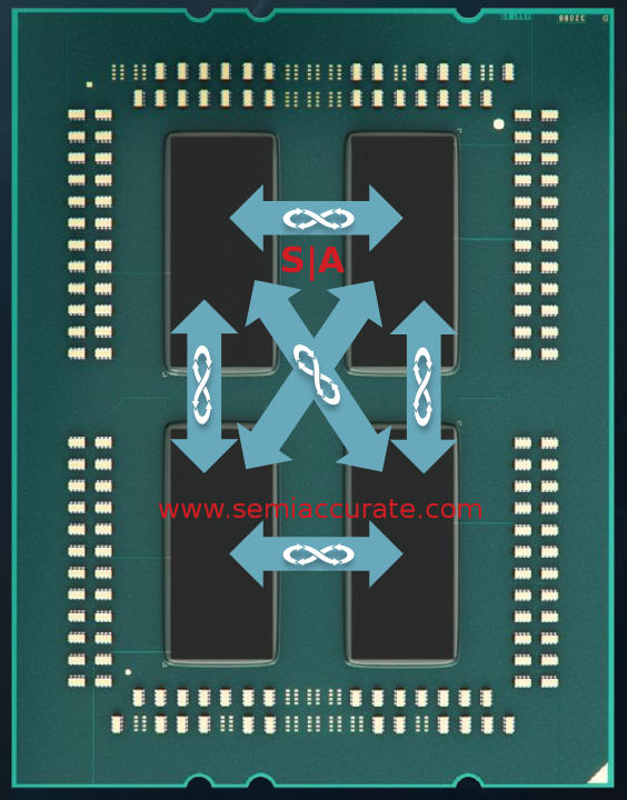
Fully interconnected Epyc MCM
AMD built Naples/Epyc in a very intelligent way, they took four die and put them on an MCM. This means much higher yields and lower costs by using four 213mm^2 die instead of a large 852mm^2 die. There is also the slight problem that an 852mm^2 die is too large for the reticle of the 14nm process AMD uses so, well, it couldn’t be made as a monolithic die even if yields weren’t a concern. We won’t go into the specifics of semiconductor manufacturing with regards to cost but lets just say AMD did it the smart way. Ignore the FUD on this front too.
Another aspect of the FUD being floated was that AMD was lashing four desktop parts together to make a second class server device. When we stopped laughing at this desperate ploy two things popped into our head. First was that the desktop Skylake-E is ‘out’ now but the server version isn’t. So if two of the Intel die chops, HCC and XCC, are ‘desktop’ enthusiast parts, what does that make Skylake-EP/Purley? If the shoe fits…
Back to the real world unpopulated by marketing an PR people, this FUD is easy to disprove by looking at the links between the dies on the package. Each of those arrows in the diagram above are 42.6GBps links, note not Gbps, and there are three per die. The dies are fully connected meaning no more than one hop between any two points on an Epyc MCM. These links and the logic behind them obviously take a significant amount of die area, something no sane company would do for a desktop part. Intel should be ashamed of even trying to float that turkey, For the pedantic the cost to move a bit between die on the MCM is ~2pj, we knew you were dying for that figure so there it is.

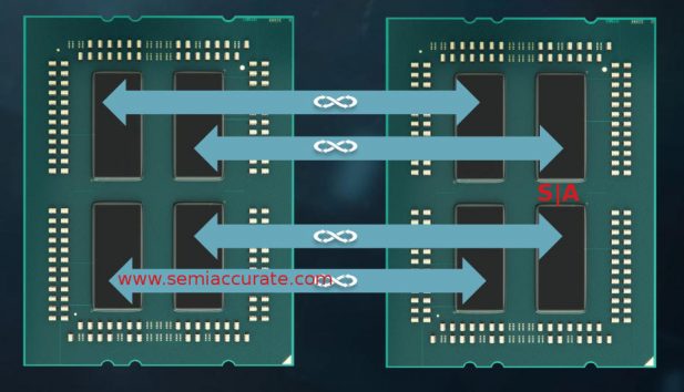
Not one but four socket to socket links
More interesting is when you look at the links between the die, they are anything but what you would expect. Rather than route everything into a single point on the MCM then across the sockets, AMD just connects the sockets with four links, one per die on the MCM. Each die is directly connected to its peer on the remote die with a 38GBps link so 152GBps between sockets. For reference Broadwell-EP has two QPI links with up to 38.4 GBps each. Assuming both are used, AMD has 2x the bandwidth between sockets as Intel’s best. This may change when Skylake-EP is revealed.
This means there are no more than two hops between any two points on a 2S Epyc system, an impressive task. SemiAccurate was told the preference is to route between sockets, then across the MCM but this may not always be the case. The cost to push a bit across the link between sockets is ~9pj per bit. The links go to the memory controller which also contains the directory cache and snoop filters and then across the die itself or to different dies on the MCM. This routing to the die rather than one CCX should significantly cut down on snoop and coherency traffic.
Technically speaking the link between sockets is less than the memory speeds so technically a single thread could swamp this link but in practice it is unlikely. Given the massive bandwidth advantage AMD has, they probably won’t run into the same QPI saturation problems Intel has but it is still theoretically possible. In short AMD has an eight die system with a two hop maximum diameter and huge bandwidth between any two points. The company wasn’t shy about calling their systems well-balanced and we agree.
More interesting but harder to quantify is the protocol that runs over all these links which AMD calls Infinity Fabric. SemiAccurate went into some detail on this link in January but the important bit isn’t any explicit spec. What is important is that AMD now has a very granular control and data fabric, separate channels mind you, that underpins their CPUs, GPUs, and anything else they end up making. IF is also transport layer agnostic so it doesn’t matter what it passes over, PCIe, die to die links, or even RFC 1149/2549 connections. While AMD did not go into explicit detail about IF and how it works, from the Epyc launch and other briefings you don’t have to dig very deep to come to the conclusion that the entire 2S system and PCIe cards can be treated as a single device. This may not do much at the moment but it is a powerful platform to build on in the near future.
Going back to an Epyc die itself, this borderline overkill connectivity is necessary because AMD is offering 128 PCIe3 lanes and 8x DDR4/2667 channels per socket, more than 2x what Intel offers on Broadwell-EP. On a 2S system 64 lanes from each socket are peeled off to form the four socket to socket PCIe3 16x links discussed above. This leaves 64 lanes per die for the user or 128 per 2S system, ironically the same number as a 1S Epyc system. Those 64 lanes are divided into four root controllers with 16 lanes each. They can subdivided those 16 lanes to eight 2x lanes max per controller or up to 32 PCIe devices per socket in a 2S machine. If you are into cryptocurrency mining platforms, your CPU has just arrived.
You might have noticed we aren’t talking about a chipset like Ryzen or Threadripper has, that is because Epyc doesn’t actually need one. Ryzen or Threadripper don’t technically need one either but the demands of a consumer platforms necessitate more I/O than Epyc offers. On die each of the four Zepplin dies has AMBus, I2C, GPIO, CLKGEN, SPI, LPC, RTC, UARTs, and 4x USB3. That last one is why the consumer parts need a chipset, 4x USB3 is laughable on a modern system. Oh yeah, SATA, some people still think this is a good thing but more importantly OEMs see it as a checkbox item. Epyc PCIe lanes can be directly used as SATA but since the external chipset tends to have them anyway, in goes a chipset even if it is not technically necessary.
So what we have here is a new CPU architecture that is modular, scales high and low, and is an actual SoC in the true sense of the term. The bandwidth between sockets is a multiple of what Intel has to offer, the memory bandwidth is 2x Intel, PCIe is 3x for 1S, >1.5x for 2S, and in general, Epyc is better at everything. It will have higher latencies for some measurements because of the modularity but most NUMA aware software and OSes should mitigate most of this. The end results will speak for themselves in benchmarks, and based on early sales information SemiAccurate has seen, AMD has a significant advantage with Epyc.S|A
Charlie Demerjian
Latest posts by Charlie Demerjian (see all)
- Nuvia Founders Have A New Startup, Nuvacore - Apr 16, 2026
- Nvidia Is Negotiating To Buy A Large PC Oriented Company - Apr 13, 2026
- Dell Does Modular Laptop Boards Right - Apr 7, 2026
- Qualcomm Snapdragon X2 Review Embargo Lifts Tomorrow Morning - Apr 6, 2026
- Intel Cuts HDR OLED Panel Power with SmartHDR - Apr 2, 2026