![]() Intel is finally launching Lakefield today but doing so in a curious manner. Briefing people after the launch is code for, “We have way too much to hide to take questions”, and unfortunately for them, SemiAccurate understands this code.
Intel is finally launching Lakefield today but doing so in a curious manner. Briefing people after the launch is code for, “We have way too much to hide to take questions”, and unfortunately for them, SemiAccurate understands this code.
Before we get in to the scant bits Intel deemed fit to gift us with before the headline grab and echo chamber effect, lets go back in time a bit. Intel had a phone SoC effort once upon a time and SemiAccurate thought it was actually a solid product.
Names like Penryn, Penwell, Saltwell, Medfield, and Moorestown are now long forgotten by the masses but they did exist, you could buy product that had them, and they were solid mid-range 3G SoCs. In a 4G world. We won’t get into the flameout of Intel’s modem business, we will merely mention that any phone ambitions at Intel are now long dead and buried.
Back to the SoCs, it was around this time when ARM announced their big.little asymmetric core designs. At one of the Intel briefings a journalist asked why Intel did not have a big.little core program like ARM did. The Intel employee who is no longer at Intel so I can tell this story replied, paraphrased, “If you make your cores right you don’t need to do such tricks. A good core can scale up and down enough to do both jobs just as well or better, and doesn’t have to have to jump through all the software hoops and play the scheduler games either.”
Today Intel brings out their first asymmetric core design and that brings up a few obvious questions. First, when did Intel forget how to make good cores? Next, will they use big.little for the name? (Spoiler: No, they are using the slightly less idiotic but still idiotic Intel Hybrid Technology and Intel Hybrid CPU architecture) Can they actually make them? Will Windows choke on the differing ISAs of the two cores? Will Intel neuter the big core to make Windows not puke? Those and many more questions may give you a hint as to why Intel is briefing the press _AFTER_ the public launch.
Back to the release today. Lakefield is finally out. It is a stacked die with memory on a 12x12x1mm package, the same size as modern cell phone SoCs if you have been paying attention. This Foveros face to face stacking, not true die stacking with vias as some might expect, is more of a 2.9D tech than a true 3D stack but considering no one else is doing it in a low volume product yet, we will give Intel that extra .1D.
Lakefield has PoP memory too and the construction allows Intel to jack the clocks up to LPDDR4X-4267 without breaking the power budget. That is a very impressive number but to get there means you can’t upgrade memory on the system. Any system that needs the board space Foveros allows won’t have a DIMM slot, trust us there. Or removable storage. In other words it will be pretty but pretty useless, just like those that covet such things.
On the core side, Lakefield has five, all single threaded. Four of these are the pretty interesting Tremont Atom cores, and one is the Ice Lake/Golden Cove ‘big’ core. All are 10nm but the big core and GPU are very likely on the 10nm high performance process while the Tremont cores and uncore are probably on a low leakage/SoC process. Again no briefing means no actual tech disclosed, another own goal.
All of these cores are single threaded in this application but the Ice core is unquestionably capable of SMT. Remember what we said about Windows puking on asymmetric cores? Any guesses why Hyperthreading was turned off here? Hint: It wasn’t to save power even if it does do so. Tremont doesn’t support AVX in any flavor so it will be interesting how much of a lowest common denominator approach Intel took to the ISAs that the Ice core supports. If our suspicions about Microsoft’s scheduler work being done by Qualcomm are correct, there is a chance AVX will be on but we doubt it for the first generation.
If they do try moving threads across cores with differing ISAs, hilarity will ensue, trust us on this one. Microsoft can’t secure a wet paper bag after 3+ decades of trying, the hard stuff like schedulers that work right is right out even if Qualcomm and ARM pitch in. If you think back to the early Hyperthreading days, Microsoft could not get the scheduler correct for that so Intel had to write one that worked and give it to them. Microsoft promptly rejected it and stuck with the terrible one they had because they feared compatibility problems. Decades later Microsoft still can’t secure Windows and is less likely to have the ability to fix real issues. If you doubt it, go look at the 3+ control panels in Windows and dig in to why they all exist.
There are two Lakefields, i3-L13G4 and i5-L16G7. If the names don’t tell you all the specs you need, here is a convenient table with all the info we have on Lakefield at the moment.
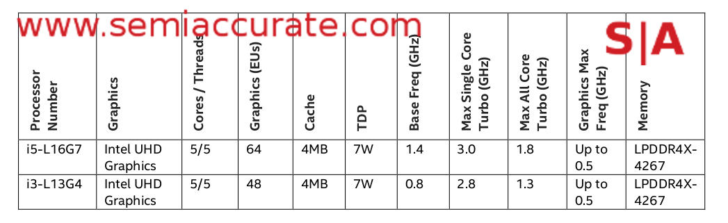
The specs in table form no less!
Lets start with the graphics, specifically the 64 EUs on the big part. This is a lot of GPU power for what is ostensibly a 7W SoC, it is effectively a full Ice Lake GPU with one working core, insert yield joke here, but it runs at a mere .5GHz max turbo. If this seems odd there is a really good reason to do things this way, power. GPUs are inherently parallel so slow and wide works just as well as fast and narrow but the latter burns a lot more power. Intel is throwing huge amounts of die area at Lakefield’s graphics to save energy and it should work really well. That said it will blow out the cost of the SoCs but Lakefield is a science project rather than a real product so who cares? If power savings are your main goal, Intel made the right choice.
When looking at display pipes things get a little odd. Intel claims there is support for up to four external monitors and video encode so it is basically a full Gen11 GPU. They then go on to say that there are two pipes to support internal monitors, likely eDP of some flavor, “making them ideally suited for foldable and dual-screen PCs.” SemiAccurate is well above quibbling about needing two pipes to support a single foldable screen but the idea that Intel is pushing dual screen devices brings back memories of speeches on how gesture recognition and other such folly were going to take over the world.
They didn’t because they inherently suck to use, something we were not shy about pointing out at the time. Dual screens mean touch panel keyboards. On a PC they are well past inherently useless, they are actively destructive to productivity and user sanity. If you are one of the few proponents of dual screen PCs with touch screen keyboards, do us all a favor and have the person reading this to you and the person explaining it to you stop immediately, then go jump in a large body of water, it will make the world a better place. If this is a portent of Intel’s ‘next big advance’ in technology, it is time to dust off the large caliber SemiAccurate combo flame/sarcasm-throwers.
Last up we come to the clock speeds, 1.4/3.0/1.8GHz base/single core peak/all core turbo for the i5, .8/2.8/1.3GHz for the i3. These aren’t bad numbers but they are not sustainable for more than a few seconds in a 7W package. It is the same PR BS from the -Y parts all over again, don’t believe it this time either but those top clocks will be achievable for a technically measurable time period. The most important thing it tells us is that Intel is nowhere close to solving their 10nm yield problems.
So in the end we have Intel launching their most advanced SoC ever. The face to face stacking is impressive, the mixed nodes are impressive, the Tremont core is impressive, and the information released is really not impressive. Taking questions only after the product launches tells us that Intel has not solved the software issues, yields are going to relegate Lakefield to a niche, and there are enough warts to make the PCs bearing the SoC expensive toys rather than functional devices. Hopefully SemiAccurate is wrong on some of these things because what we know about the underlying tech is quite interesting.S|A
Charlie Demerjian
Latest posts by Charlie Demerjian (see all)
- Intel Bumps Xeon Memory Speeds - Jul 20, 2026
- Qualcomm’s 2026 Investor Day Has Hidden Goodies - Jul 15, 2026
- Phison Phudges The Numbers… In A Good Way - Jun 24, 2026
- Who Are The Qualcomm Enterprise Customers? - Jun 23, 2026
- Innodisk Adds 10GbE To Useless M.2 Slots - Jun 19, 2026