![]() Intel is finally talking about 14nm and the results are impressive, both in terms of transistors and yield. That said it is both just a claim and not out yet but lets take a look at what we will hopefully see later this year.
Intel is finally talking about 14nm and the results are impressive, both in terms of transistors and yield. That said it is both just a claim and not out yet but lets take a look at what we will hopefully see later this year.
The first point to make is that the process name is “14nm” as opposed to the “22nm” process that preceded it. What are those numbers? In the past they referred to minimum drawable feature size but that world is long gone, Intel says it hasn’t been the case since the 90nm days or so. If the nm in the name does not refer to a physical dimension, what does it refer to?
Process naming is and has been for quite a while a reference to the shrink factor of the new node compared to its predecessor. In short this means if a 130nm process has a minimum drawn feature size of 130nm and a cell size of X, a shrink is going to be half the cell size. This means a 90nm process should have a feature size of 90nm and a cell size of X/2.
From 22nm to 14nm cells shrink 2x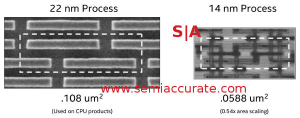
Intel has said that around 90nm that linear feature size path stopped mostly because we are still on 193nm light sources and have to use tricks like double patterning to fake the rest. You can make smaller drawn features but it may not make sense to do so anymore especially considering the move to 3D/FinFET structures. The train we are on now is that the minimum drawn feature size many not scale directly but the minimum cell size somehow ends up being half that of its predecessor.
How? Who cares as long as it works. In short a shrink from A -> B no longer means the minimum drawn feature size conforms to (A^2) = 2(B^2) but a cell size of X on process A will be X/2 on process B. That is the key, the area used by a cell halves but the how changes and does not necessarily track to a specific factor like minimum drawn feature size. This is why SemiAccurate and others are annoyed by Samsung, Global Foundries, and TSMC calling their ‘shrink’ from 20nm ’16nm’. What they are delivering is a 20nm process with planar transistors replaced by FinFETs but the Back End of Line (BEoL) or metal layers barely changes. That means almost no effective shrink, Samsung is claiming between a 7% and 15% for their 20nm to their 14nm nodes.
Such shrinks are more in line with a normal mid-life process optimization than a real shrink from 20nm to 16nm. This is the long way of saying other than Intel’s, no 14/16nm process is an actual shrink from 20nm planar, cell size does not come close to the theoretical (20^2)/(16^2) shrink factor, it is almost non-existent. If Intel does deliver what they claim, we buy the naming of their “14nm” process, the rest are effectively slinging a load of BS to the non-technical masses this generation.
With that in mind what is Intel delivering this round? If you look back to the 22nm days, Intel was very quiet about important dimensions like aspect ratios. 14nm changes some of that but not everything. The first thing to take into account are the three main metrics governing transistors, Fin Pitch, Gate Pitch, and Interconnect Pitch. These three factors went from 60 to 42nm, 90 to 70nm, and 80 to 52nm in the move from 22nm to 14nm. Those would be scaling factors of .70x, .78x, and .65x respectively.
Since you need a roughly .7x 1D scaling factor across the board to get X/2 area scaling for a cell, Intel is right there. The biggest bang comes from one point, the Interconnect Pitch scaling of .65x or 80nm to 52nm, the first change in that metric for quite a while. Why? 80nm is the smallest feature size you can draw with single patterning, 52nm requires double patterning on the metal layers. This adds a large amount of process steps adding time, cost, and yield loss, something no company wants to do unless they have to. Intel has to scale 22nm -> 14nm so they smiled and double patterned. Although we asked, Intel would not say how many layers of 52nm interconnects their process supports but Mark Bohr did narrow it down to between 1-13 layers. This Interconnect Pitch shrink is both the bulk of shrink and a necessity to make the new process work.
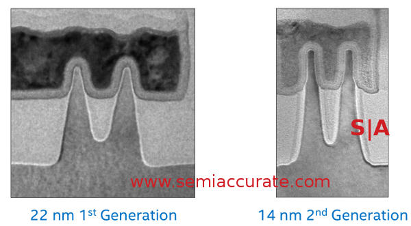
Note the angles of the fins on each
One more number to throw out at you, 42nm. This is not the same 42nm as the 14nm process Fin Pitch, it is the Fin height, an increase from the 34nm heights in the 22nm process. In semiconductors, almost any increase in size is a bad thing but in this case it is very good. One of the key factors in transistor performance is contacted gate area which is determined by physical area in planar transistors, fin height and length in fins. This means if you want a contacted gate area of X and you have a height of Y, you need to have a length of X/(2Y).
That in turn means if you want more performance you need to make the transistor longer at a linear area cost or make it taller for ‘free’ performance. Since fin height is fixed for a process, changing that really isn’t an option at a given node. Worse yet this is probably one of the hardest things to do well in a FinFET, just look at the wall angle on the 22nm process for a good example. Worse yet the fin aspect ratio is about 3:1, not very large.
This all changes at 14nm, the walls of the fins are almost planar, vastly more so than those on 22nm. They are also closer together, 42nm vs 60nm so the contacted gate area goes way way up. (Please note we are ignoring the contacted gate area of the top of the fin for simplicity, it is slightly more for the 22nm process but not all that much more.) This allows Intel to get much better performance from the same length transistor, the same performance for a much shorter length transistor, or something in between. Since shorter is directly related to area used per transistor, height is directly related to the shrink factor.
One more very important change is what Intel calls Fin Depopulation (FD). The idea is that the basic building block of a 22nm transistor was three fins. Due to the improved performance of the 14nm fin through all the mechanisms mentioned above and more, you don’t need three fins to do the same work. If you can do the same job with two 14nm fins, you can drop one and make the same circuits with far less area over and above the normal areal scaling factors. While FD is not technically a process metric, the net result is the ability to pack far more transistors in a given area while doing the same work. Please note that this is not taken into account in the transistor scaling from 22nm to 14nm, it is over and above the 2x scaling factor from that.
That brings us to the last point, yield. Designing a process that has amazing metrics for shrink, performance, and all the rest is an easy task on paper, actually making them in volume is not quite so trivial. As you can tell from the timeliness of Intel’s 14nm product stack, they are having the proverbial ‘issues’ with the first chips coming out roughly a year after they were expected. Worse yet, something seems amiss with the result, two things really but Intel denied both problems.
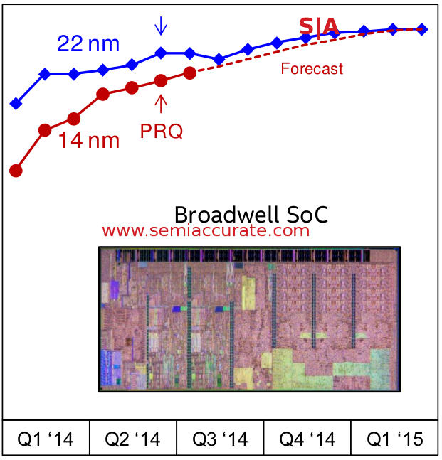
Note the projections vs data
Intel is claiming that their 14nm process is on track, the process is PRQ’d now, and production is ramping. There are two things to notice about the yield chart above, first is that although the Y-Axis is number free, it is clear that 14nm is yielding at a far lower level than 22nm, the rest are projections not data. This directly correlates with other data that SemiAccurate has received over the past several months.
More interesting is the second point, there isn’t the traditional comparison to more than one process, just the last. Intel does claim that their 22nm process is the best they have ever done at least using defect density as the performance metric. This is likely true but numbers from non-public sources that SemiAccurate was told say that the end result does not match that single metric. We will leave things at that.
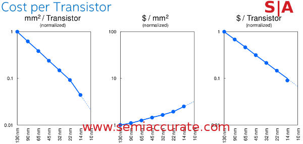
Cost curve assumes constant defect density
The end result is that the transistors Intel makes at 14nm are significantly smaller than 22nm, roughly half of the area and cost less than the traditional scale factor would suggest. This also means that while wafer cost undoubtedly goes up, cost per transistors plummets. Intel did say that these charts assumed a constant defect density rather than actual yields so technically the result should be better than shown if they are correct about yields. Also note that the charts are logarithmic.
Regardless of the yields, performance is definitely better. The contacted gate area goes way up so in theory leakage goes down while performance goes up. Intel can pack almost twice as many transistors in a given area as before than and they work better than before. Although the minimum drawn feature size is nowhere near 14nm, the scaling factor is quite real and in line with expectations. In short this 14nm process is really a step forward, others can’t make that claim.S|A
Have you signed up for our newsletter yet?
Did you know that you can access all our past subscription-only articles with a simple Student Membership for 100 USD per year? If you want in-depth analysis and exclusive exclusives, we don’t make the news, we just report it so there is no guarantee when exclusives are added to the Professional level but that’s where you’ll find the deep dive analysis.
Charlie Demerjian
Latest posts by Charlie Demerjian (see all)
- Intel Bumps Xeon Memory Speeds - Jul 20, 2026
- Qualcomm’s 2026 Investor Day Has Hidden Goodies - Jul 15, 2026
- Phison Phudges The Numbers… In A Good Way - Jun 24, 2026
- Who Are The Qualcomm Enterprise Customers? - Jun 23, 2026
- Innodisk Adds 10GbE To Useless M.2 Slots - Jun 19, 2026