![]() ARM was talking up their TSMC 10nm Artemis test chip last week with some juicy details. There wasn’t much about the core performance directly but the process bits are definitely good stuff.
ARM was talking up their TSMC 10nm Artemis test chip last week with some juicy details. There wasn’t much about the core performance directly but the process bits are definitely good stuff.
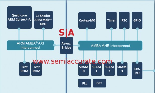
You might recall when SemiAccurate first brought you the news of Artemis about 1.5 years ago, we got the marketing name wrong but the rest pretty close. Last October ARM announced a collaboration with TSMC on 10nm chips and today we can tell you about the first product of that pairing. It goes by the hip marketing name, “TSMC 10nm FinFET Test Chip” and has four Artemis cores and one GPU block specifically mentioned to not be Mimir but it is a high-end gaming part. In addition you have a slew of interconnects, a Cortex-M0, bridges, SRAMs, ROMs, and all the rest. The block diagram looks like this.

All the bits and more
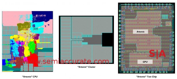
If you want to see the more detailed plots and block diagrams of the cores, they are below. One thing to make note of is the far right layout, note the size of the four cores vs a 1x GPU cluster, it puts an interesting perspective on things.

More versions of the test chip
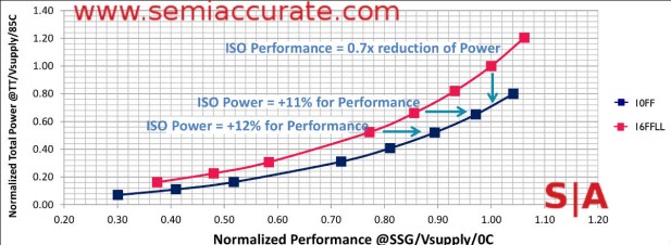
That brings us to what you get from the shrink, basically how TSMC’s 10nm process stacks up against their 16nm process. The three points on the graph below were picked to roughly correspond to normal, overdrive and super-overdrive points for the 16nm process. You can see the results of a shrink to 10nm, not a clean kill but solid gains on the power or performance fronts.

TSMC 16nm vs 10nm voltage curves (Note: Data from ARM not TSMC)
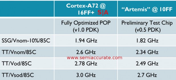
So what exactly does that work out to be in real numbers? ARM was nice enough to put that out in table format for us, or at least a variation of it with A72@16nm vs Artemis@10nm. Different cores, different processes, and most important a fully baked PDK for the A72 vs a v0.5 PDK for Artemis. Once thee PDK matures the 10nm numbers should go up significantly and ARM expects Artemis on 16nm to be significantly higher frequency than A72. For the record the voltages for 10/16nm are .75/.8V for nominal, .85/.9V overdrive, and 1.0/1.0V for super-overdrive.

The diagram in table form
As you might expect, Artemis is looking like a better core than A72 and 10nm is a little better than 16nm but nowhere near a full shrink’s worth of progress. Rather than end it there we will throw out a few tidbits we learned about the process and related tech.
First is cost, and it goes way up for 10nm. A design that cost about $5M on 28nm is said to rise to a bit over $30M on 10nm, a bit more than a linear rise. When you see presentations bemoaning the cost of lower geometries, this is what they are talking about but as usual, your mileage will vary. Part of this rise is that 10nm uses triple patterning which will not only increase costs but also increase the time it takes to run a wafer by more than a little bit.
Update May 18, 2016@11am: $5M cost was for 28nm, not 16nm, fixed.
Last up is something we weren’t expecting, starting at 14nm ARM implemented stage based variation. What this means, vastly simplified, is in the past you needed to buy a timing margin on all transistors in a stage which effectively slowed down the whole device for increased yield. At 14nm that margin is implemented on the first transistor in a stage and it is decreased with each successive transistor in that stage. How much is a bit of a black art but having it decrease makes for a better and smaller chip. This carries over into 10nm and you should see some of this in the numbers when Artemis is outed in more detail.S|A
Charlie Demerjian
Latest posts by Charlie Demerjian (see all)
- Nuvia Founders Have A New Startup, Nuvacore - Apr 16, 2026
- Nvidia Is Negotiating To Buy A Large PC Oriented Company - Apr 13, 2026
- Dell Does Modular Laptop Boards Right - Apr 7, 2026
- Qualcomm Snapdragon X2 Review Embargo Lifts Tomorrow Morning - Apr 6, 2026
- Intel Cuts HDR OLED Panel Power with SmartHDR - Apr 2, 2026