![]() Today Intel announced an eight wavelength silicon laser device that pushes the boundaries of optical communications. SemiAccurate has been following Intel’s optical efforts for quite a while and it is good to see them talking about something close to production.
Today Intel announced an eight wavelength silicon laser device that pushes the boundaries of optical communications. SemiAccurate has been following Intel’s optical efforts for quite a while and it is good to see them talking about something close to production.
The main focus of today’s announcement is an eight wavelength distributed feedback (DFB) on chip laser device. While this specific chip isn’t going to be productized, the process of making it and the related technologies will be soon enough. The device itself consists of four major parts, a silicon multi-wavelength laser, micro-ring modulators, silicon photodetectors, and semiconductor optical amplifiers. All of these things are challenging to make on their own so Intel claiming high yields on a device with all four is very impressive. Lets look at what they do and more importantly how they fit into the chips Intel makes.
Advanced packaging with lasers
The lasers are made at a dedicated Intel 300mm InPh fab so tooling and volume is going to see a lot of cost benefits versus smaller wafers with more exotic tooling. In short think economies of scale. The current test device has two groups of four lasers who’s output is then grouped into pairs, pairs again, and pairs again for a single output stream over a single fiber. Think 8 -> 4 -> 2 -> 1 but the diagrams we were given are just bad renders, sorry. While Intel did not want to talk about products, current 4-fiber PSM4 QSFP devices and single fiber 4-wavelength CWDM4 QSFP devices both run at 100Gbps. Any guesses what speeds Intel is targeting this 8-wavelength device at?
Intel’s silicon lasers, ring modulators, amplifiers, and detectors have all been proven in the field so the basic tech is already there in volume on currently available products. The problem now is that when you add more lasers, modulation, etc to the mix, you generate more heat. Heat and optics don’t play well together, higher temperatures lower output and cause frequencies to drift.
The industry has a multi-source agreement, basically the relevant vendors all get together and agree on guidelines for power and wavelength uniformity at each generation. This time around there is a +/- 1dB power uniformity target and a +/- 50GHz frequency target. On this early silicon, Intel achieved +/- .25 dB on power and +/- 13GHz frequency tolerances. Assuming production parts will get better as volume ramps and feedback comes in, Intel seems to be in a pretty good place with this eight laser structure. For absolute numbers, Intel has a channel spacing of 200GHz +/- 13GHz.
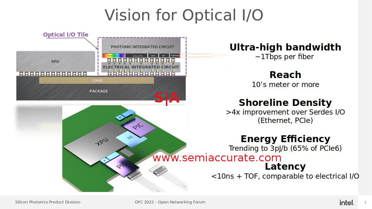
So why is Intel doing this when you can just run the same data over electrical connections without the hassle of optical, InPh processes, and all the rest? Power. Moving data is becoming the critical bottleneck in modern compute for both bandwidth and energy use. You can do what Intel is proposing for this eight laser device across copper but it will be for meters while optical has a reach of kilometers. The current devices are claimed to use <3pJ per bit while doing the same over PCIe6 will need about 50% more energy and just can’t go more than a few meters if you are lucky.
That brings up the thorny question of cost which Intel rightly claimed isn’t just the cost of the laser and related components, all of which are likely more expensive than their electrical counterparts. If you use electrical connections at these speeds you need to use low loss materials which cost quite a bit, go look at the cost of PCIe4 vs PCIe5 motherboards for more on that. If you take the entire data path into account, optical isn’t out of line with electrical for costs. Add in reach and lower energy use and things swing towards optical even more. The industry is at a crossover point for communications, if optical isn’t the clear winner now it will be by the next generation which is why Intel is pushing this eight wavelength device now.
Moving on to the most pertinent bit is how Intel is going to integrate this laser device into their product line. Making optical transceivers is the obvious one but SemiAccurate thinks that is the least interesting case. You still have to drive those bits off the chip, across a (likely) PCIe bus, and then onto the NIC which is both slow and energy intensive. If you couple the laser to the die generating the data across a silicon bridge or interposer, those issues go away, as does a lot of the cost. If you look at the diagram above, this is exactly what Intel is proposing.
The construction starts with the aforementioned eight wavelength DFB laser and modulation structures built at the Intel InPh fab. This device is <1.5mm x <1.5mm in size and it is face to face (F2F) bonded to a standard silicon wafer which houses the control logic and electrical I/O. From there you can put it in a transceiver package or more likely on to an advanced packaging setup with a silicon bridge to the data generator. Intel will almost assuredly offer this as a tile for their foundry offering in the not so distant future but they would not comment on productization plans for the time being.
So in the end, what is Intel putting out today? An tight tolerance eight wavelength DFB laser communications test device that will be the heart of their upcoming 200Gbps NIC line. Because of how it can be packaged, it is likely going to be the basis for their on package chiplet/tile die to die direct communications strategy too, and that is far more interesting than the next step in PCIe cards. Since the whole device is based on current production technologies, we don’t see much standing in the way of a full product rollout either, bring on the 200Gbps optical era.S|A
Charlie Demerjian
Latest posts by Charlie Demerjian (see all)
- Intel Bumps Xeon Memory Speeds - Jul 20, 2026
- Qualcomm’s 2026 Investor Day Has Hidden Goodies - Jul 15, 2026
- Phison Phudges The Numbers… In A Good Way - Jun 24, 2026
- Who Are The Qualcomm Enterprise Customers? - Jun 23, 2026
- Innodisk Adds 10GbE To Useless M.2 Slots - Jun 19, 2026