 Qualcomm’s 2026 investor Day had a lot of goodies, and a lot of questionable claims. SemiAccurate will dive into some of the high points and try to give you a little more background on the technical claims.
Since we are hardware focused, we will start out with that, then move on to some of the statements we can’t abide by, and finish with a little finance. There is a lot of the proverbial good, bad, and ugly here although not necessarily in that order. The hardware hints are vague as promised but you can cross-reference a lot. Unfortunately the footnotes and expected disclosures were woefully absent as is par for the course at Qualcomm. Finance had one customer disclosed, Meta, but SemiAccurate disclosed that and one more a few days prior.
2H/2028 has a lot of meaning
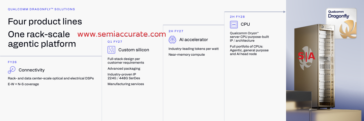
The stage was set by Tony Pialis early on with a roadmap that is pretty much what SemiAccurate expected. This year Qualcomm enterprise hardware sales are more or less the Alphawave SerDes customers, a company Qualcomm acquired a few months ago. This is fine but none of it is intrinsically Qualcomm, take that as you will.
In FY27, Q1 in fact, Qualcomm adds advanced packaging and ‘Manufacturing services’, whatever those may be. The slide above makes vague references that they are moving from “E-W + N-S coverage” to “Full-stack design per customer requirements”. What this means is that they are going from making optical and copper interconnects that connect standard rack servers to an integrated network design ala Nvidia or AMD’s Helios.
The TLDR is that instead of making point to point interconnects, Qualcomm is going to make a system that hopefully turns a rack into a single unit. Same basic tech, just arranged in a different way. And yes we know it isn’t that easy but the analogy holds. It is also likely to have precious little Qualcomm input at the moment, this is almost assuredly Alphawave’s doing.
Big numbers, vague specs
The next part is an “AI Accelerator” in 2H27 followed by a CPU in 2H28. We will dive into each in a bit but first comes the big bang of the day, a new ‘tech’ called HBC or High Bandwidth Compute. This tech, scare quotes above for a reason, is not really new tech or much tech at all. Before we get into why SemiAccurate thinks this, take a look at a pretty diagram of the product.
This HBM diagram is Slide 10
Note the substrate and bottom die on Slide 11
(Note: Slide 10 and 11 were placed that way for a reason)
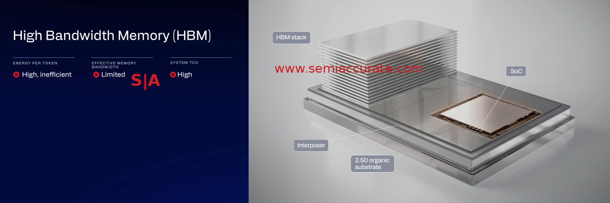
So what do we have here? One slide earlier, Qualcomm dissed HBM memory as having high energy per token, limited effective memory bandwidth, and high system TCO. These are fair criticisms of HBM but is HBM an HBC competitor? Qualcomm sure wants you to think so but this is disingenuous at best. HBM is a pure memory stack meant for high bandwidth vs traditional DIMMs or GDDR, HBC is a complete accelerator. HBM can’t do any compute, HBC can. It is like comparing a dump truck to a Ferrari and trashing the Ferrari because it can’t haul 12 ton boulders. True but fair? Comparing an accelerator subsystem to a memory chip is… just wrong.
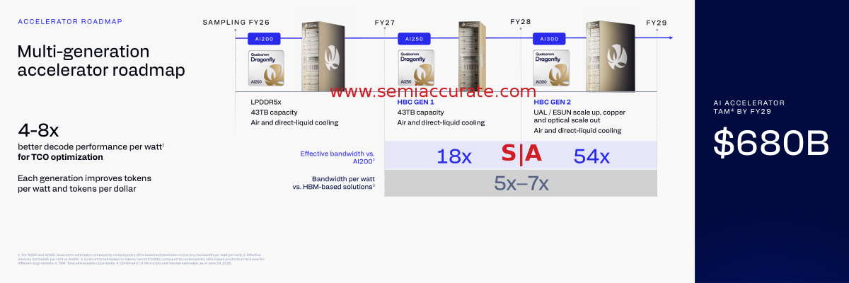
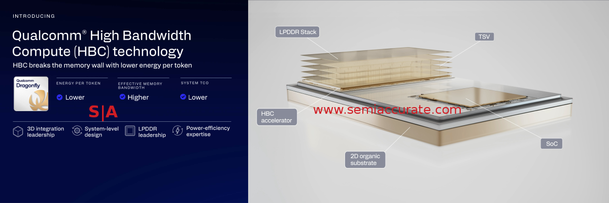
At this point you are probably wondering what HBC is, and why Qualcomm wants you to compare it to HBM. What it is is easy enough, take an AI accelerator, in this case AI250 but Qualcomm won’t say that, and place a stack of LPDDR5 on top of it. It could be massively efficient for memory access and the claimed 18x bandwidth improvement over AI200’s external LPDDR5x is quite plausible. All good so far.
The SoC is just the main system CPU so HBC is directly attached and soldered down to the board or more likely daughter card. Take note of the 2.5D organic substrate part, this is a big Qualcomm talking point but it is just a tradeoff. Organic substrates are vastly cheaper than silicon bridges/EMIB or worse yet interposers but they also have down sides. The bump pitch is significantly coarser so the memory bus width is far narrower and slower than a silicon interconnect. Organic also leaks more and the thicker traces eat more energy, this is the long way of saying that silicon interconnects are much more efficient per bit. Qualcomm took the tradeoff to use organic substrates and LPDDRx rather than silicon and HBM but it is a choice between tradeoffs, nothing more. This isn’t good or bad but the messaging is disingenuous, more on that later.
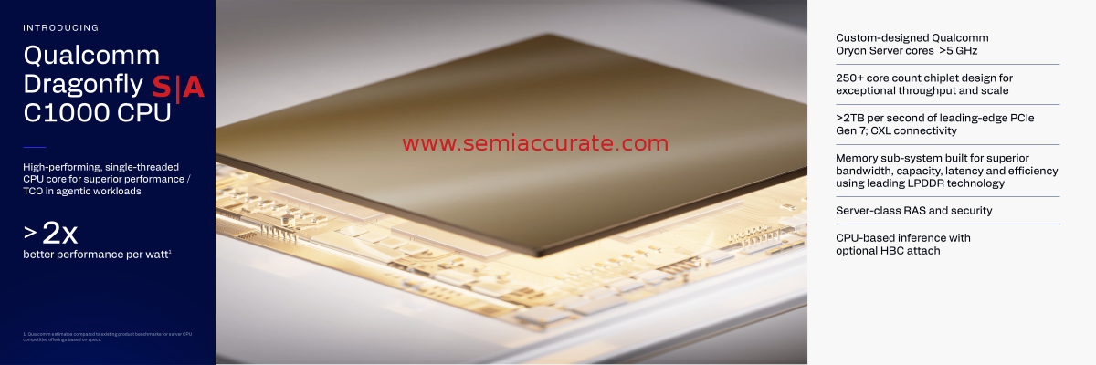
Qualcomm’s new C1000 CPU in vague terms
From there we move on to 2H/28 and the new CPU architecture, purportedly purpose built for servers. It is called the Dragonfly C1000 and it is single threaded, a rather curious choice for the intended market. If you are wondering why we say this, just ask Intel how well their single threaded server chips did on the market, it wasn’t pretty and Intel backpedaled after a single generation of this painful and costly mistake. Qualcomm is going to have the same issues for the same reasons but those are mostly out of the scope of this article. *****Put link to intel’s issues**
One thing SemiAccurate can’t ignore is the rather unethical claim of “>2X better performance per watt”. Why? If you look at the footnote, it says, “Qualcomm estimates compared to existing product benchmarks for server CPU competitive offerings based on specs.” Lets break that down a bit in detail because the magnitude of the, “They really stooped that low?” rockets it to the top few questionable statements of the last decade.
First lets look at times. The C1000 is due in 2H/28 if all goes well, and we will assume it does for now. Server CPUs are ~3 year projects from clean sheet to product on the shelf, often times more but we will stick with the best case. 2H/28 minus 3 years is 2H/25 so that is about when the project started. What also happened at Qualcomm in 2H/25? The key architects for the Qualcomm cores and SoCs all quit. Some stayed and the exodus didn’t become public until February 2026, but the brains behind the current cores were gone quarters earlier. They have since founded Nuvacore to also make cores, something that shocked no-one. This isn’t to say that Qualcomm has no people left but the brains they touted so loudly are gone. Who is the new team? No clue. :)
So it is a new team making the C1000, we have no view on their competence but a few months in to the program, it is interesting they have numbers already for a design that is quarters away from the architecture being finalized to be built on a process that is 2+ years from being ready. That said we will assume they have a clue about their targets and will hit them. Why is this still a problem?
Well the fine print says they are comparing the C1000 to EXISTING products and the phrase, “Qualcomm estimates” triggers more alarm bells than SemiAccurate knew it had. Then they do the usual Qualcomm disclosure trick of claiming it against benchmarks but not naming them. Think they cherry picked the good ones or perhaps made up new ones that favored them? Would they do such a thing?
Then there is the issue of a 2+ year out product being compared to current devices. Do you think AMD, Intel, and Nvidia will advance their product lines in the next few years? There is one AMD product, Verano, on the roadmap in that time that will advance efficiency far more than the linear curve of semiconductor progress may intone. That >2x for C1000 is not going to age well, this is a know, not a guess. As time goes on, this slide will haunt Qualcomm, it was an extremely poor choice that should not have been allowed to make it to the public presentations.
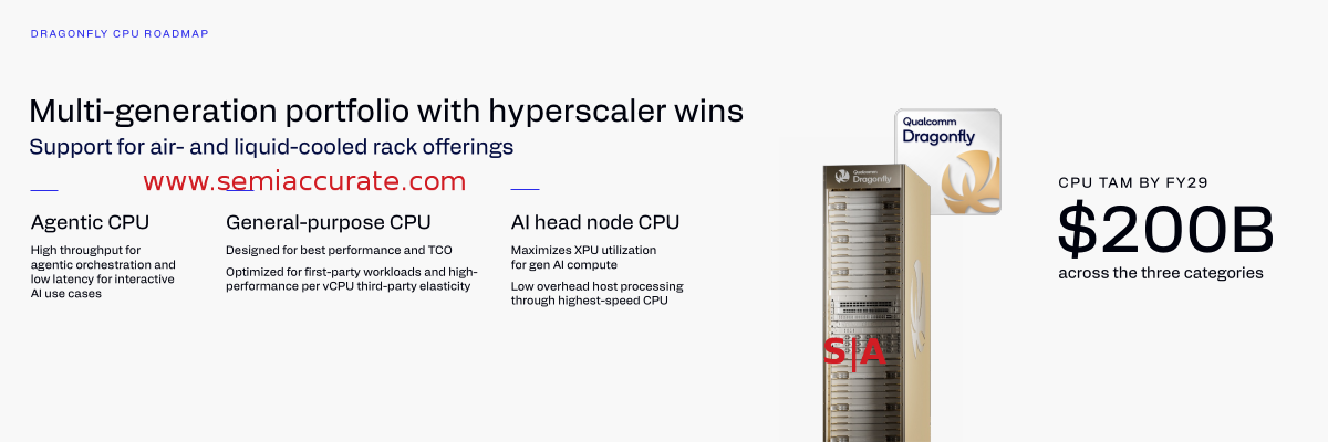
Three CPU types are coming in 2H/28
Back to the tech we have a few more hints on the next slide with three types of CPUs listed, agentic, general-purpose, and AI head node. The last two are the easiest, one is a generic CPU ala AMD and Intel but with a skewed I/O:compute ratio, basically how many cores per PCIe lane. AI head nodes are essentially glorified bootloaders, remember Qualcomm signed the Nvidia NVLink trojan license, and the general CPUs lack this functionality. Since the NVLink ‘license’ is just a UCIe link and communication protocol, you have a pretty clear path to how Qualcomm is going to implement their chiplet strategy, just substitute a standards based I/O UCIe chiplet and you have the general-purpose CPU.
The agentic version is similar, take some core chiplets out and slap on an AI based chiplet. There is an off chance that Qualcomm will spin a different core with tightly coupled AI accelerators on each chiplet like the current consumer devices but we consider this a bit unlikely for the first generation. In any case, a UCIe based chiplet design can do all three flavors of CPU with a minimum building block count. Any guesses as to what the interconnect to the AI250/HBC accelerator is going to be?
Last up we have to comment on the, “250+ core count chiplet design for exceptional throughput and scale” from the C1000 slide. The most pressing question is, how many cores does Qualcomm mean by 250+? Could it be 255? Dare to dream it could be 257? 83? No, not that, but 256 single threaded cores is not going to look very impressive against AMD or Intel’s current offerings much less their 2H/28 offerings. AMD’s Venice will have 256 cores with two threads THIS YEAR and they aren’t stopping there. Downclocking a Venice to the optimal PPW point should have vastly superior throughput to the C1000 and it is available soon. Then there is AMD’s Verano we mentioned above. Oh yeah, don’t forget AMD’s ‘small’ cores either.
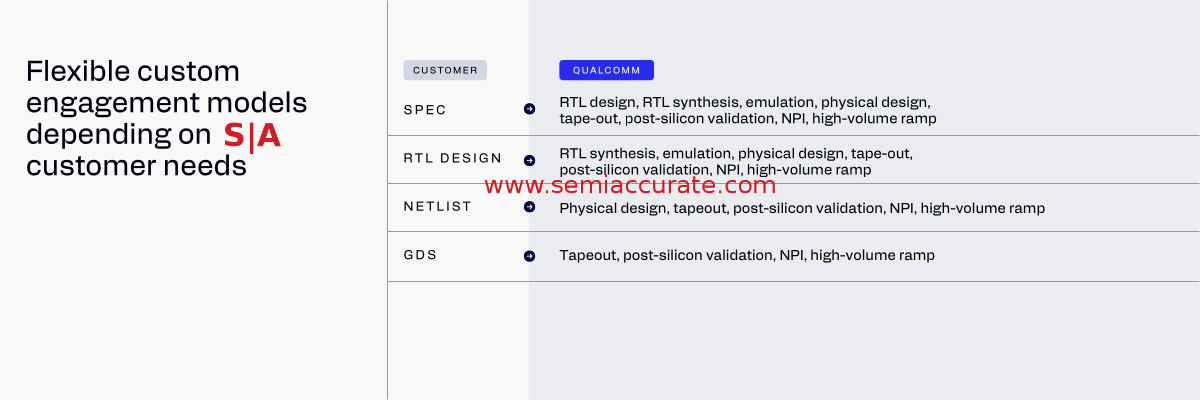
This is a new product category for Qualcomm
Last up on the technical side we have the new offering of custom silicon projects, essentially Qualcomm is in the semi-custom business now and they have one of the best people in the industry to lean on there. The pitch is pretty standard but the last one rang alarm bells, small ones, not the symphony from above. We read Qualcomm’s GDS line as saying, “We have lots of wafers that we have paid for but can’t fill. Want to buy them?” Before you pooh-pooh that logic, this is the exact pitch Qualcomm is making to potential AI customers as we said a few days before the event.
So as a whole, what is Qualcomm’s enterprise hardware lineup? For now it is Alphawave’s roadmap, same with next year. In late 2028 we have the first Qualcomm core but it is from a new team, not the existing Nuvia/X Elite/Nuvacore guys. This isn’t to say it won’t be good, it could very well be spectacular, there isn’t any way to judge yet. Take an AI200, put a stack of LPDDRx on top of it, add a UCIe interface and voila, you have an ‘HBC’ accelerator. This is the optional AI accelerator called AI250 and AI300 wrapped in a marketing term. Throw in semi-custom CPUs and SoCs via the UCIe interface and chiplet designs, and you have the slate of Qualcomm enterprise offerings. In 2H/28. Unless there is something spectacular SemiAccurate missed here, it is going to have a really tough time competing with existing AMD and Nvidia products not to mention the near future stuff. That said, game on.
Now back to those pesky statements we can’t abide by. A few were covered above, the >2x bit and the HBM comparisons. Lets look a bit more at the HBC vs HBM ‘debate’, again different classes of device that bear no relationship to each other. Take a close look at the table for efficiency on the roadmap slide above, the one that claims, “4-8x better decode performance per watt.” The fine print says this is compared against contemporary GPU architectures. GPUs are not known for their efficiency, they are brute force designs that go fast and take a lot of power to do so. They are also external devices so the power to push the bits across a PCIe bus or worse yet NVLink is not trivial, but they are fast.
That comparison is again a bit less honest than we are comfortable with but the worst part is, “decode performance”. Decode? Decoding what? Compared to what? Guess what wasn’t disclosed? But again it is 2H/28 hardware vs current hardware. *SIGH*. Qualcomm should do better than this.
Then there is the table that lists effective bandwidth of the AI250 and AI300 at 18x and 54x the AI200 respectively. This isn’t a stretch to believe going from an external LPDDRx bus to a TSV based stack does widen the bus width dramatically, a multiple like that, coupled with a generational improvement of the memory makes that 18x an easy target. The 54x for the AI300 generation is basically a 3x generational advance, think double the bus width and a little faster memory. So far so good.
Then there is the, “5x-7x better bandwidth per watt vs HBM-based solutions” claim. Hear those alarm bells again, you can’t miss them. HBM is not meant for efficiency, it is meant for speed first, efficiency second. Nvidia makes both HBM based solutions and LPDDRx based solutions for AI. Guess which one is higher performance? Guess which one is more efficient? Qualcomm COULD have compared their LPDDRx offerings against the Nvidia LPDDRx based offerings, it is on the market and Qualcomm almost assuredly has them in their competitive intelligence labs.
So why didn’t they? You could give them a pass and say they claim their products are competing against the Nvidia HBM products, not the LPDDRx ones, but that doesn’t hold water. The Nvidia HBM products are training products, the LPDDRx lines are aimed more at inference. That said both can do either job but Qualcomm’s lineup is inference heavy. This whole claim, while technically defensible, is about as close to dishonest as you can slide past legal. Then look at the memory capacity numbers for the Dragonfly racks and work the numbers back. I hear 2020 servers calling. No, 2018, 2020 had those numbers in the rearview mirror.

Rack diversity is not news
That brings us to the topic of disaggregation, Qualcomm says that we are now in an era of all-in-one racks and training optimized datacenters. The future is inference-optimized and disaggregated. This is absolutely true, sort of. Anyone who has any clue about modern data centers will know they are currently all disaggregated and have been for many years. Facebook was giving talks about this at Hot Chips pre-Covid as were many others. It is not new, no modern datacenter could function with an early 2000’s monoculture of racks. Why Qualcomm thinks that this is the case now and AI will suddenly bring about a change is beyond us. It takes us back to the early cloud days when the definition of cloud was, “what we have to sell”.
Then there the something that is not specific to Qualcomm but they seem to be using it above and beyond the call of duty, tokens. Not tokens themselves but using ‘token’ as a performance metric. When AI hardware was first being foisted on the PC space by Microsoft fiat, TOPS became the currency to measure performance by. Everyone in the industry decried using TOPS as a metric but Microsoft MDF depended on hitting 40 TOPS so everyone used it. It meant nothing because while it did measure raw numerical capability, it was almost utterly divorced from what performance was actually achievable. TOPS was and is useless for anything but marketing to the uneducated.
Tokens are much the same. If someone says, “We can do XYZ tokens per second and our competitors can only do half that”, which one is better? If your tokens result in a 34% correct answer on average but the other guys do 98% at half the speed, which is better? Using ‘token’ as a performance metric without qualifiers is useless, comparing 100 tokens/second on a 500 million parameter model vs 10 tokens/second on a 5 trillion parameter model is pointless. We should probably take another dig at Qualcomm’s lack of proper disclosure here but that would seem petty. Back to the point, tokens per second can have uses but it is NOT a generic metric to compare disparate things against each other. If you tied it to the exact workload and benchmark, maybe, but Qualcomm and most others don’t. Please stop.
Then we come to the elephant in the room, finance. Qualcomm was more than happy to tout massive numbers for the datacenter TAM, $1+ trillion in 2029, GASP! SemiAccurate’s position is that AI demand has peaked and finance is a lagging indicator, but lets take Qualcomm at their word and assume their numbers will happen. A $1T TAM in 2029 means what for Qualcomm? They announced Meta as a customer at Investor Day, SemiAccurate announced Meta and another days earlier.
Our research indicates there are currently no CPU customers for the C1000 but some are likely due to the Alphawave and interconnect ties. Others are interested because of the wafer availability pitch linked previously. So there is a huge TAM and Qualcomm has two big potential customers, but there is one catch, even assuming both sign up for the C1000, what will it bring Qualcomm and why? Industry sources told us one important detail about how contracts like this are framed which could radically change the numbers.
Note: The following is analysis for professional level subscribers only.
Disclosures: Charlie Demerjian and Stone Arch Networking Services, Inc. have no consulting relationships, investment relationships, or hold any investment positions with any of the companies mentioned in this report.


Charlie Demerjian
Latest posts by Charlie Demerjian (see all)
- When Is Nvidia releasing N1X/Spark Systems? - Oct 2, 2026
- Qualcomm Finally Fixes Their PC CPU Line! - Oct 1, 2026
- What Is Intel’s Diamond Rapids Server CPU? - Sep 11, 2026
- ARM’s 2026 ‘Tech’ Day Is A Self-Inflicted Wound - Sep 7, 2026
- Intel Bumps Xeon Memory Speeds - Jul 20, 2026
