 AMD is launching three new technologies today, four if you count like SemiAccurate does. V-Cache comes to servers in Milan-X, ROCm gets an update, and GPUs go dual-die with advanced packaging.
The first of the items is the one that will likely grab all the headlines is Milan-X, basically the consumer 3D V-Cache on servers. If you don’t know what V-Cache is, read this. In short it is a 64MB SRAM/cache chip that is mounted on the top of each CCD bringing the total L3 per ‘die’ to 96MB or 3x that of the 32MB base CCD. That means a fully fleshed out Milan-X will have 768MB of L3, a borderline insane number. On the technical side, AMD says the latency of the L3 will increase by about 10% with the added cache die but the capacity multiple is more than worth it.
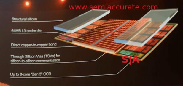
Note the spacers
For some applications it will be a massive boost, AMD quotes a 66% uplift on Synopsys VCS performance, on others it will barely make a difference. This is the long way of saying if your workload benefits, it is probably a program with large licensing costs so Milan-X is a no-brainier. If your workload doesn’t benefit much, it probably isn’t worth the (presumably significant) extra cash so stick with Milan. Yes we know this wasn’t a huge leap of logic but we had to say it.
There were a few interesting technical bits in the briefing on Milan-X starting with the fact that AMD admitted that the pads for the V-Cache were in Rome, something Semiaccurate has been saying for a while now. Then there are the bumps or more to the point copper pillars. V-Cache uses a copper to copper direct bond, solderless, and likely an alloy that bonds on physical contact at this scale. It is a very simple and elegant bit of advanced rocket science.
The last bit was possibly the most revealing, SemiAcccurate asked why they didn’t cover the whole die rather than putting silicon spacers on each side of the cache. There were several answers starting out with 3x L3 is a lot to how much more costs, the cache die is on the same process as the CCD. Then came the real reason, heat. If you notice on the floor plan of the CCD, the cache is in the middle while the cores are on the outer edges. AMD wisely placed the heat sensitive bits of the V-Cache away from the hot cores for higher performance, again a smart thing to do.
About the only bad thing we can say about the V-Cache is that AMD is doing the stupid marketing trick of adding the L1 and L2 to the L3 and giving “total cache per socket”. There is no need to do this, it is idiotic and makes you look stupid to the very technical crowd this part is aimed at. Just stop it, really, for your own good and our blood pressure. KTHANKSBYE.
Moving on to the software side, AMD is announcing ROCm 5.0 which is one better than the previous best ROCm 4.0. It adds support for the new MI200 GPU line, more code bases and libraries, and better everything but no big bangs. Getting with the times, AMD is also opening a new portal for the ROCm enthusiast called the AMD Infinity Hub at https://amd.com/infinityhub. As of this writing there is no MI200 or ROCm 5.0 info there but we presume it will be live by the time you read this far down.
MI200 posts some big numbers
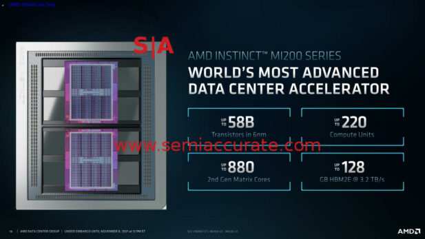
That brings us to the next hardware goodie AMD is announcing today, the MI200 GPU in both OAM and PCIe formats. There are two OAM devices, the MI250 and MI250X which top out at 550W, and the PCIe card based MI210 which probably pulls a lot less. These GPUs appear to be FP64 heavy and FP16/BF16 light plus the lack of Int numbers points to a potential sore point. That said the 3.2TBps of memory bandwidth is pretty good but falls a bit short of the per-die bandwidth of the A100 it is compared to. If your app needs FP32 or FP64, these are the cards for you. If you need Int8 or Int16, you might want to test before you spend.
MI200 is all about the advanced packaging
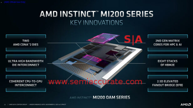
That brings us to what SemiAccurate feels is the most important announcement of the day, the construction of the MI200 package. As you can see above there is a lot going on so lets break it down for you. The MI200 is basically two GPUs on a large package-like structure. Each of these packages is a mix of things but not a substrate in the conventional sense. Each die is connected by four links between them, likely Infinity Fabric over PCIe4. These are then mounted to a larger conventional package that has the spacer/stiffening ring on it. So far so normal, sort of, mostly.
You might recall that the eight HBM packages usually require an interposer for the traces, an expensive way to connect dies. Intel stepped out of the box with EMIB and only put in a tiny piece of silicon interposer that just connects only the parts that need to be connected. It is cheaper than an interposer in most cases but requires the substrate manufacturer to jump through a lot of hoops. As you might have guessed the MI200 has no interposer and no EMIB so what did AMD do?
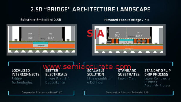
EFB is second generation EMIB
The mostly conventional substrate that the MI200 dies are mounted to is a very high end but otherwise conventional substrate package with an embedded bridge that AMD calls EFB or 2.5D Elevated Fanout Bridge. It is like EMIB in many ways but a lot more elegant in most. That said they more or less do the same job but how they get to the end point is the noteworthy part.
For EMIB, Intel fabs the bidge on an older node, think 65/90+nm rather than 14/22nm, and sends it to the packaging house. The packaging house lays down some of the substrate core layers and then laser etches a cavity in the part. The EMIB bridge is then placed in it and the rest of the layers are built up around the bridge. It works, is likely ready for high volume, and most if not all of the multi-hop alignment bugs have been worked out. That said there are no consumer volume mass market devices on the market with EMIB yet but SemiAccurate doesn’t see this as an indicator of anything amiss.
AMD’s approach is far more elegant in many ways. They take the wafer on wafer bonding approach that TSMC and many OSATs have been doing for years now and place the bridges like any other 3D bonded semiconductor, think stacked TSV memory and the like. The rest of the structures around the bridge are then built up around the bridges and cut out leaving a structure that is the exact size needed. This structure, bridges, GPU, and HBM are placed on a conventional substrate package and all is good.
AMD calls this lithographically defined bridges because it uses the same lithographic techniques to make the structure that you use to make a stacked chip. It is more precise and less fraught with ‘whoopsies’ that drop yields than ablating cavities in substrates with a high powered laser. That said AMD has none of these devices on the market at all, high volume or low, so yields and manufacturability are up in the air. EMIB is completely viable, EFB probably is too but we will have to wait and see.
Note: The following is for professional and student level subscribers.
Disclosures: Charlie Demerjian and Stone Arch Networking Services, Inc. have no consulting relationships, investment relationships, or hold any investment positions with any of the companies mentioned in this report.
Charlie Demerjian
Latest posts by Charlie Demerjian (see all)
- Intel Bumps Xeon Memory Speeds - Jul 20, 2026
- Qualcomm’s 2026 Investor Day Has Hidden Goodies - Jul 15, 2026
- Phison Phudges The Numbers… In A Good Way - Jun 24, 2026
- Who Are The Qualcomm Enterprise Customers? - Jun 23, 2026
- Innodisk Adds 10GbE To Useless M.2 Slots - Jun 19, 2026